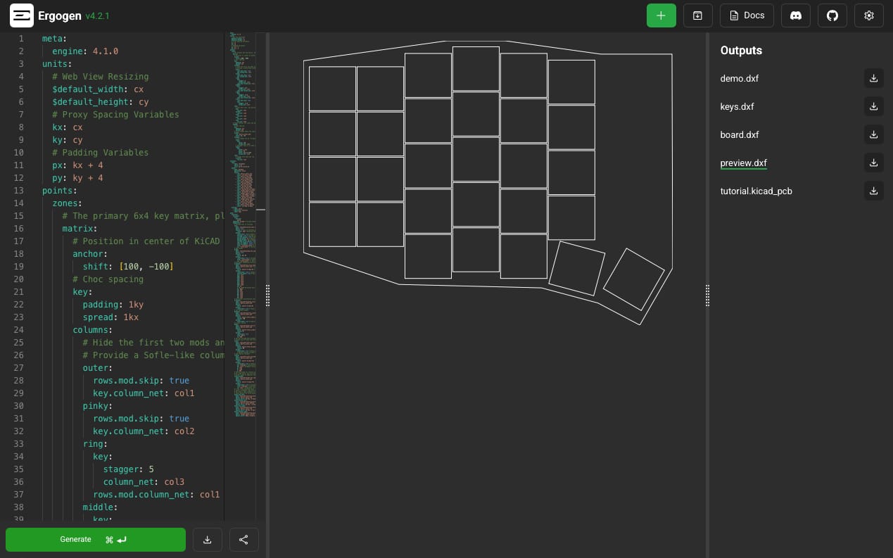
It's hard to believe that it's been three years since I wrapped up Let's Design a Keyboard with Ergogen v4. Since posting that original guide, the most persistent question I've received is, "When are you going to make a chapter on reversible split keyboards?" Well the long wait is over. The time is now.
Sort of. Split keyboards are a big topic. The reason I went with a unibody keyboard for the original Let's Design guide was that it kept the number of variables to a minimum. The complexity of a design build starts ballooning out when you split the keyboard across multiple halves. There's also the small matter of I haven't designed that many split keyboards. I've created two wireless split keyboards based around my goofy TypePak cartridge, but those aren't the most tutorializable builds.
So this writeup is going to be more of a collection of tips than a step-by-step guide. If you're starting from scratch, Let's Design a Keyboard with Ergogen v4 is still where you want to begin. Once you know how Ergogen works and how to finish up your build in KiCAD, this article will point you in the right direction when it comes to making a split keyboard. Come back here once you have an understanding of Ergogen's Points, Outlines, PCBs, Footprints, and wiring everything up in KiCAD. Ergogen itself has also been updated a bit since that original guide, so I'll also briefly touch on some of the larger improvements.
Split Keyboard Basics
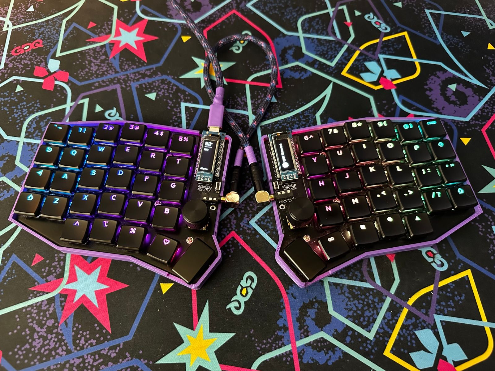
A split keyboard is just what it sounds like: It's a keyboard made up of two distinct halves. You can place them wherever you'd like on your desk, and get a bit of a more ergonomic experience without having to "bow" your arms together.
Rather than presenting themselves as two distinct keyboards to your computer, the left and right halves typically communicate with each other first before finally exposing themselves as one single USB or Bluetooth keyboard. This allows the two halves of the keyboard to more easily behave like a single keyboard. You can press the Right Shift key on one half of your keyboard and the A key on the other half of your keyboard, and a capital A will appear in your text prompt.
The way that this usually works is that you have a "Primary" keyboard half and a "Secondary" keyboard half. The secondary half reports its physical state (which buttons are being pressed, etc.) to the primary half, and then the primary half is exclusively the piece of hardware which communicates with your computer. There are typically ways of specifying with your keyboard firmware which half is the primary and which is the secondary. The early Let's Split keyboard's firmware defaulted to left for the primary half, and right for the secondary half, and most subsequent builds followed this convention. (Thanks for digging up that research Drashna!)
The "Primary" and "Secondary" terminology is becoming somewhat anachronistic. Some keyboards have multiple non-primary parts, so "Secondary" is a clunky term to refer to them. The wireless ZMK firmware uses the term “Central” and “Peripheral” to describe its split parts. I probably should have adopted that terminology here, but I had already drafted significant portions of this guide using the older terms, and I didn't want a Find-and-Replace to go wrong.
Wired or Wireless?
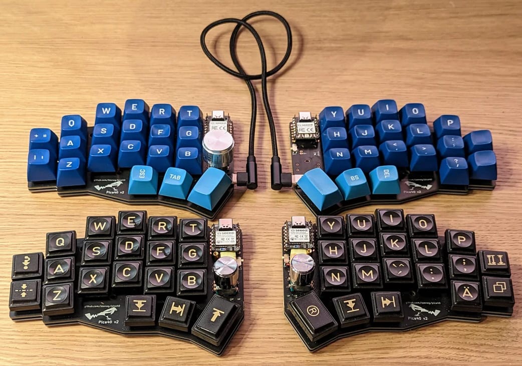
The biggest consideration one needs to make when building a split keyboard is whether it's going to be wired or wireless.
Wired keyboards use a USB cable to connect the primary half with the computer, and then a second cable of some kind to connect the primary and secondary halves. The absence of any batteries or wireless technology typically makes them cheaper to build and more logistically straightforward to design, build, and use. You'll never find yourself halfway through a sentence unable to type a J due to your right half's battery suddenly dying. Wired keyboards also get to dabble a bit more freely in fancy LED effects since they're not concerned about the light show's effect on battery life.
Wireless keyboards meanwhile typically use Bluetooth to communicate. The primary half and your computer leverage Bluetooth to send keyboard signals, and the primary and secondary halves usually use a wireless connection to discuss their own current state. Wireless keyboards look a bit more clean on one's desk, and can often be easier to travel with. They often have multiple Bluetooth profiles as well, allowing you to rapidly switch between Bluetooth devices. There are some concerns when working with wireless DIY keyboards, but those are typically limited to the device's battery life. Wireless keyboards usually have a USB fallback option, allowing the primary half and your computer to communicate over a wired connection. This allows you to press F12 easily during a BIOS boot screen on a retro computer, and can mitigate some concerns about latency during PC gaming.
I’m having to use words like “typically” and “usually” a lot in this section. Counterintuitively, one of the first things you want to think about when designing new keyboard hardware is what software it’s going to run. The various open source keyboard firmwares support different microcontrollers, and have limitations or quirks which will drive the overall part selection and capabilities of your split keyboard.
You can of course program a microcontroller from scratch, but writing your own keyboard firmware is a bit outside of the scope of this guide. For the rest of this guide I’m going to assume you’re using QMK for wired keyboards, and ZMK for wireless keyboards. There are some other great options out there like KMK and RMK, but QMK and ZMK are what most DIY keyboards are based around at the moment.
Wired Split Keyboards with QMK
QMK is the perennial open source keyboard firmware. It's been around for ages, supports a wide range of hardware, and is widely adopted by the DIY community and keyboard vendors alike. There are even some GUI options like VIA and Vial to let you remap your keyboard without having to get up to your elbows in config files. QMK's focus has largely stayed on wired keyboards. As such, it remains the best option for power-hungry components like animated RGB LEDs or large LCD screens.
When it comes to building a split keyboard with QMK, there are only two big decisions you need to make: Which microcontroller are you going to use, and how are the two halves going to connect to each other.
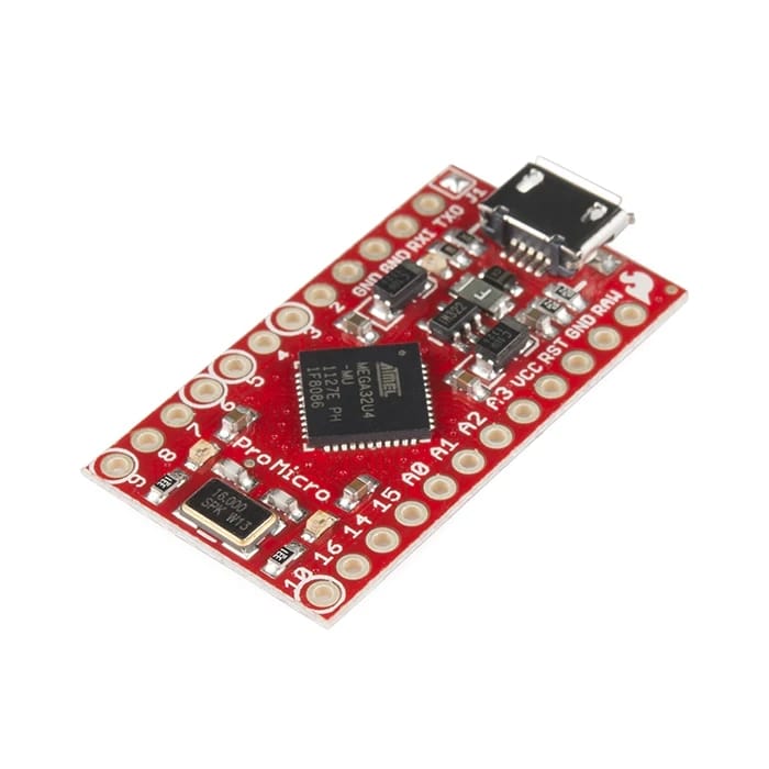
QMK supports a few different types of microcontrollers. Early QMK builds were designed around the "Arduino Pro Micro". This was an open source microcontroller developed by Sparkfun and powered by an 8-bit ATmega32U4. The ATmega32U4 still works with QMK, but it has a small memory footprint that users can easily hit when dabbling with QMK's more advanced functionality.
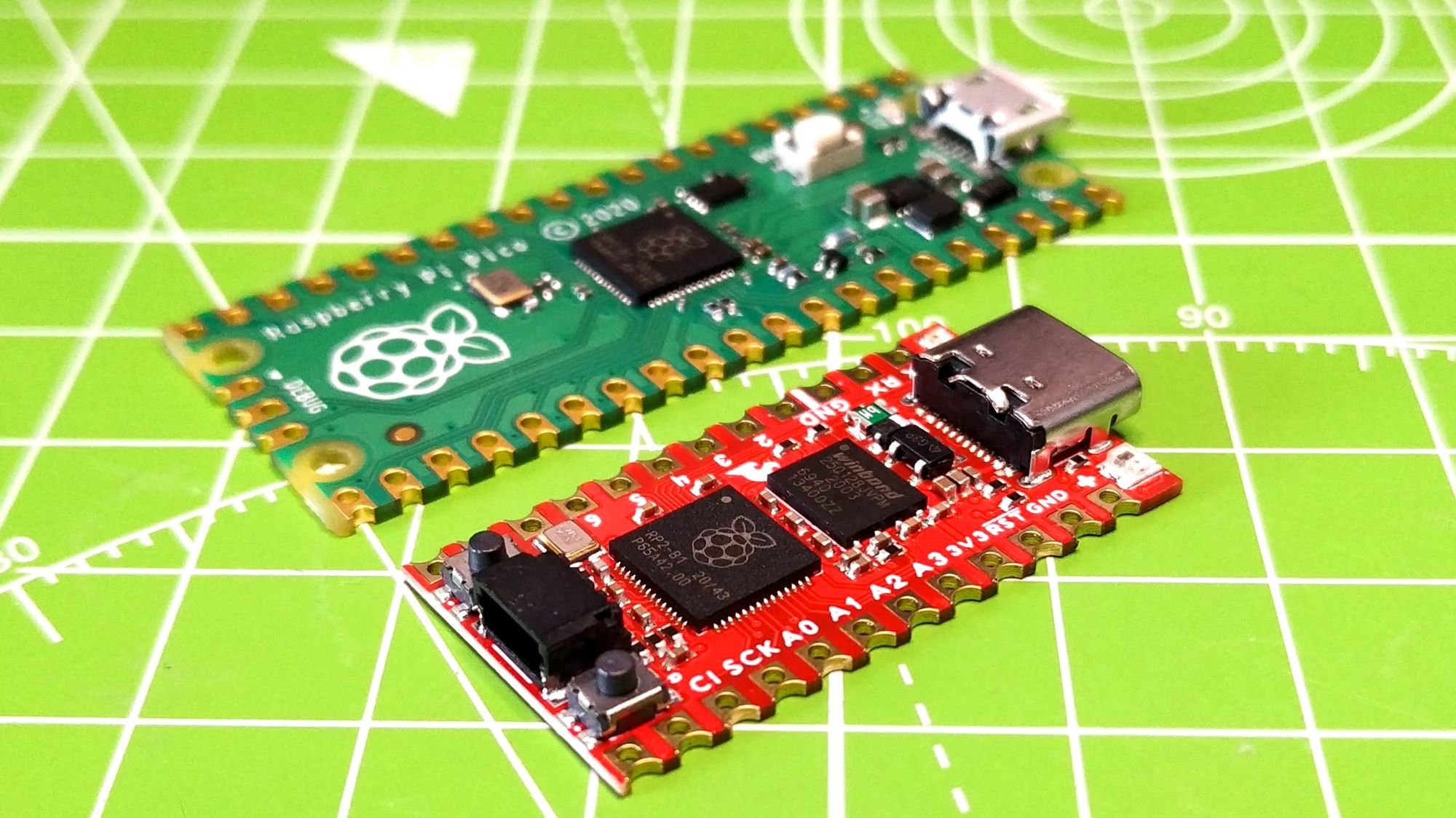
For more modern builds, you typically want a 32-bit microcontroller with a bit more horsepower behind it. The community dabbled for a while with STM32 based microcontrollers, but has largely rallied around the popular and affordable RP2040 microcontroller. The RP2040 is the heart of the Raspberry Pi Pico. This development board was designed to be a cheap and modern alternative to the aging Arduino platform.
In the context of DIY keyboards however, the Raspberry Pi Pico is a relatively large microcontroller. Thankfully several vendors have created RP2040-powered microcontrollers in the same size and pinout as the classic Arduino Pro Micro. These microcontrollers like the Elite Pi or Frood are a drop-in replacement for any board designed to work with a Pro Micro. QMK has a more expanded list of RP2040 Pro Micros, but there are also plenty of generic options out there. Just typing, "RP2040 Pro Micro" into Amazon or Aliexpress should find you something suitable.
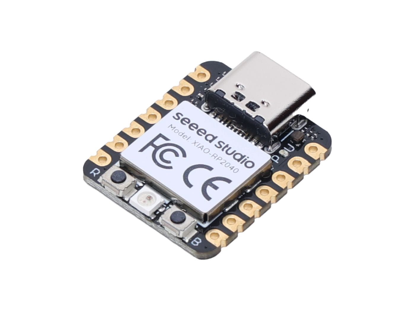
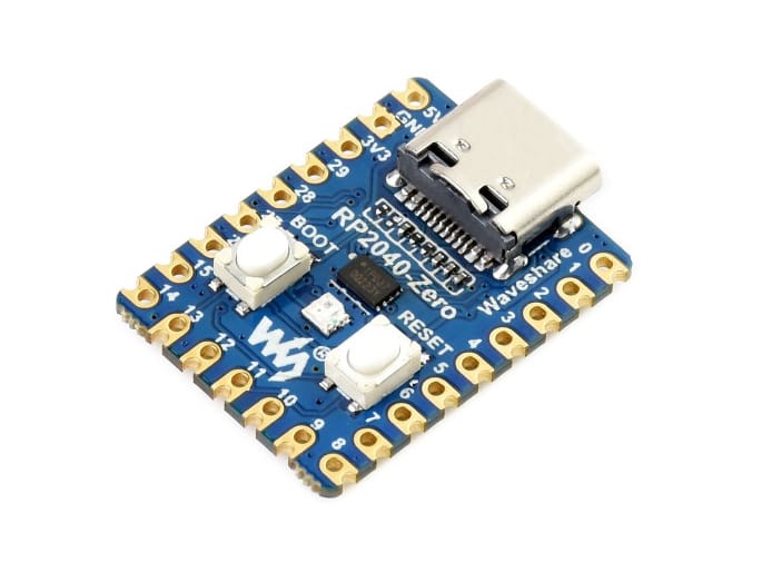
Outside of the Pro Micro form factor, Seeed Studio's XIAO line of boards is popular for smaller keyboards. (Macropads, etc.) It includes a nice compact RP2040 variant. The Waveshare RP2040-Zero is also a popular option for an in-between microcontroller with a small size but a good amount of pins.
Whichever microcontroller you go with, you're going to need two of them. QMK uses a dedicated microcontroller for each half of the keyboard. They deal with scanning the keyboard matrix, registering button states, and dealing with any other accessories like LEDs or LCD screens. The built-in USB port on the primary half's microcontroller is what eventually gets connected to the computer. The USB port on the secondary half's microcontroller remains unplugged.
When setting up the keyboard's firmware, QMK will output two files: One for the primary half, the other for the secondary half. Again, the convention is to have the left half be the primary, but you can set it up with the right half as the primary if you make a few tweaks to your config.
The two microcontrollers need to communicate somehow, which means you're going to need some wires connecting the two halves. Right from the get-go, you need to supply power to the microcontroller on the secondary half. That means the cable connecting the two sides will have at least a VCC power wire and a GND ground wire. On top of that, you'll need some additional wires for the two microcontrollers to actually communicate over.
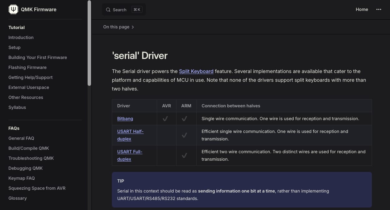
QMK supports two serial communication protocols for communicating between split halves: Bitbang and UART. (For communicating with serial peripherals, QMK also supports I2C and SPI.)
Bitbanging is QMK's default option. It uses a single wire which the two microcontrollers use to send serial data back and forth on. It can use any GPIO pin on your microcontroller. There's a bit more overhead on your microcontrollers to keep the back and forth timings right.
UART meanwhile can use one wire "Half Duplex" or two wire "Full Duplex" modes. Half duplex leverages a single serial wire similar to bit-banging. Full duplex meanwhile uses a pair of serial wires. In Full Duplex mode, the TX transmit pin on your primary microcontroller connects to the RX receive pin on your secondary microcontroller. Meanwhile the RX pin on your primary microcontroller connects to the TX pin on your secondary microcontroller.
I recommend consulting the QMK documentation to make sure you've got the proper serial setup for whichever hardware combination you decide to leverage. There are a few quirks, such as half duplex UART requiring a pull-up resistor unless you're using an RP2040. Additionally, using bitbanging to connect the two halves of your keyboard doesn't play nice with the popular WS2812 RGB LEDs.
Whatever you decide to go with, you're going to need a power wire, a ground wire, and one or two serial wires connecting your two microcontrollers. You could just permanently solder a few loose wires between your two keyboard halves, but most builders want something a bit more polished and a bit less permanent. Thankfully we've got a lot of cables and connectors to work with.
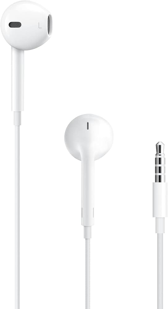
Most beginners gravitate towards 3.5mm headphone style "TRRS" cables. These are the plugs you see on headphones which also have an inline remote or microphone. (iPhone wired earbuds, etc.) TRRS stands for Tip-Ring-Ring-Sleeve. Each segment of the connector carries one signal, so we can use it for both bit banging or UART. The classic headphone connector without the microphone/remote is just a TRS connector since it only has one ring.
TRRS jacks are easy through hole components to solder. You can put the power connections at the far ends, and the serial communication in the middle. They're nice and durable, and there's plenty of good looking options of varying lengths. The one thing you need to be careful about is not connecting or disconnecting a TRRS cable while a keyboard's plugged into USB. The connectors weren't designed to carry power, so there's a chance you could bridge something you shouldn't.
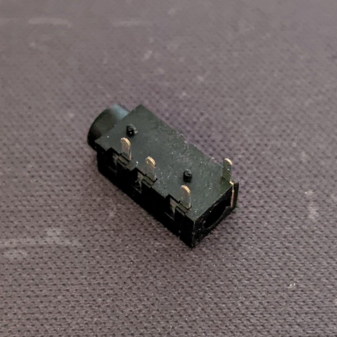
The other popular alternative is plain old USB. Classic USB cables have four wires in them, and these connectors were made with power in mind. So there's less of a chance they'll short out your secondary microcontroller. Additionally, there's plenty of nice cable options out there. You can use whichever type of USB connector you'd like, with the modern USB-C being the most popular option.
The type of connector you use is largely inconsequential as long as it can safely carry the power and serial data to your secondary microcontroller. People have dabbled with RJ45 ethernet jacks, FPC ribbon cables, magnetic header pins, etc. Your choice of a headphone jack or USB-C largely comes down to your personal preference and soldering skill confidence.
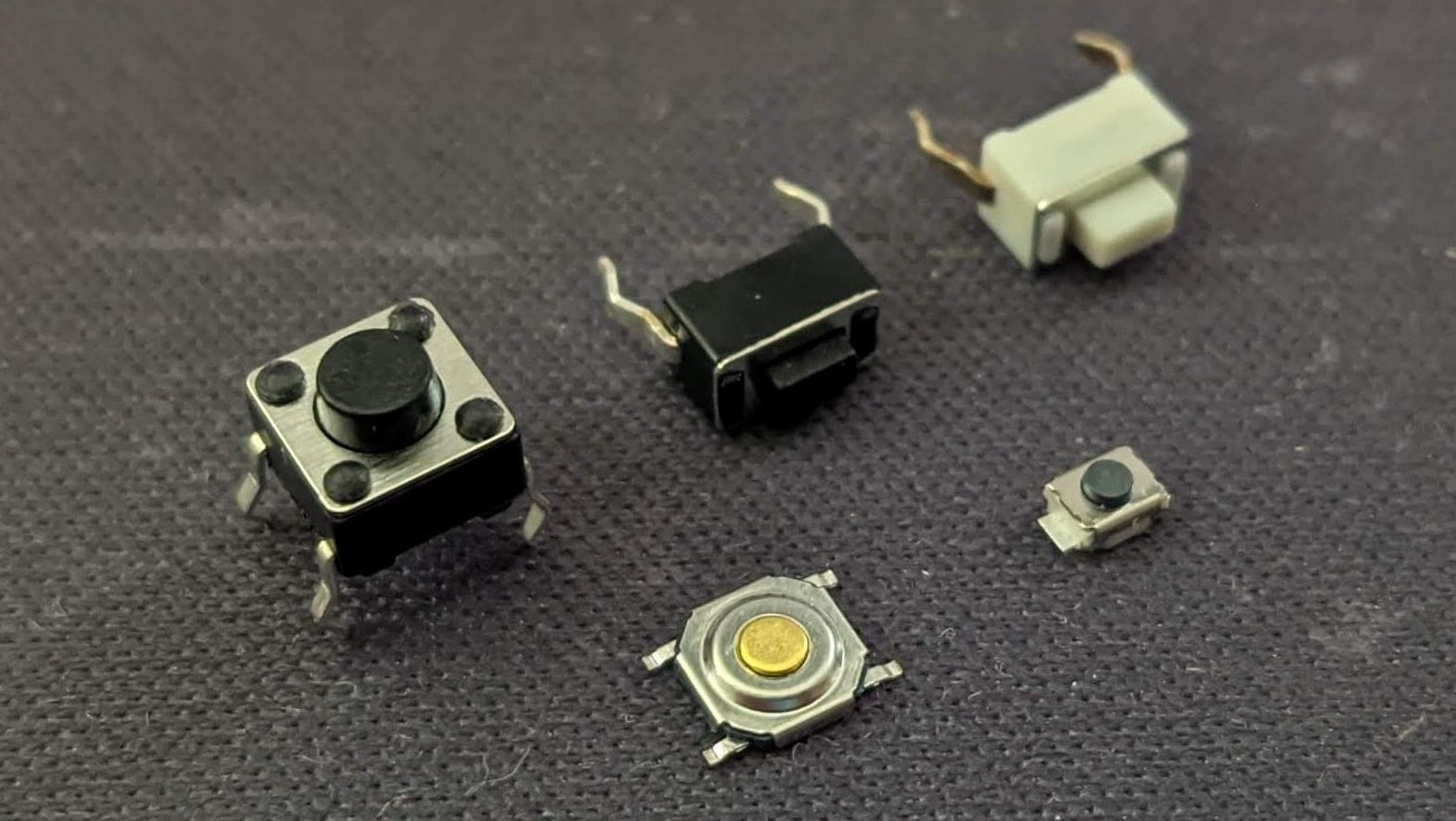
In addition to the microcontroller and split keyboard cable connection, you'll usually want to include a small pushbutton for resetting your microcontroller. Some microcontrollers have a button built in, but adding one to your keyboard makes it less fiddly to flash with a new firmware.
What about those wired keyboards with only one microcontroller?
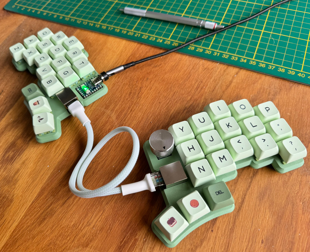
You'll occasionally see keyboards with an RP2040 on their primary side, and a distressing lack of any microcontroller on their secondary half. These builds are getting exceptionally creative with their wiring.
The common TRRS and 4-wire USB ports are not the only connector option out there. USB-C offers a variety of wires depending on the port and cable type. RJ45 networking connectors have eight built in wires. Flat FPC ribbon cables have a variable amount of wires traveling through them.
Depending on your cable type, you could have enough wires to build your matrix on the second half of your keyboard without relying on a second microcontroller. An RJ45 cable can provide 16 keys with a standard 4x4 matrix. You can eke out even more with some non-standard Charlieplexed matrixes like the Cheapino uses. Things get even more ambitious if you add additional components such as a shift register. With just 4 wires, a shift register can give you 8 additional column pins. Suddenly your secondary RJ45 connected half can have 32 additional keys.
Under the hood, these "split" keyboards are technically designed like a unibody keyboard with very unusual wiring.
These techniques are fairly uncommon however. The secondary half would be difficult to use with any advanced components such as an LCD screen, LEDs, or other common keyboard accessories. RP2040 Pro Micros aren't excessively expensive, so pulling off these sorts of tricks is usually more trouble than it's worth. Where you occasionally see them crop up is in triple-split keyboards. QMK's software only supports two halves in a split keyboard.. Dangling a number pad off of your secondary half and treating it technically like an ordinary shift register allows you to have the aesthetics of three pieces without having to get too complicated on the software side of things. Again though, these builds are rare to the point that it's almost not worth mentioning. I just included a mention for completeness' sake.
Wireless Split Keyboards with ZMK
Now for the piece you're probably here for! Wireless keyboards are having a bit of a moment in the DIY keyboard building space. Ever since the Nice!Nano microcontroller and ZMK firmware burst onto the scene, it’s been easier than ever to build a truly split keyboard. There's a few more considerations to take care of however, but we'll start with the firmware and microcontroller selection.
ZMK is a newer open source keyboard firmware that is a bit younger than QMK. It's evolved by leaps and bounds over these last few years however. It supports an increasingly large pool of hardware, and has a nice code-free configurator in the form of ZMK Studio. In my opinion, the project's also just overall easier to work with. ZMK even offers Github Actions so that you don't need to set up a complex build environment locally.
The firmware primarily targets the nRF52840 microcontroller. It's a low power Bluetooth chip available in a few different form factors. ZMK also has support for the notably non-wireless RP2040 and STM32 microcontrollers. Again, ZMK is nice to work with, so even some wired builds are beginning to adopt it now.
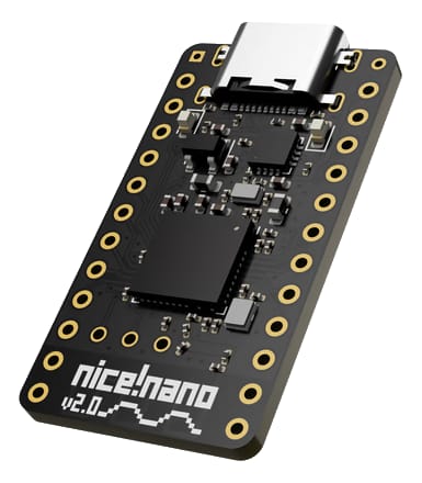
The Nice!Nano microcontroller really got the ball rolling on the popularity of nRF52840 microcontrollers. It's in the classic Pro Micro layout, and offers a few additional niceties which allow it to serve as a drop-in replacement for wired PCBs with the traditional Arduino/RP2040 Pro Micro in mind.
The first of these added aspects most people notice are a small pair of Bat+ and Bat- pins at the top of the Nice!Nano. These pins are spaced out of step with the other header pins in both spacing and size. They're not meant to be included with the microcontroller's typical headers or inserted into the keyboard's socket. Instead these pins allow you to add a Nice!Nano to an old PCB design which was created without the Nice!Nano in mind. By soldering a battery directly to these Bat+ and Bat- pins, you can power your Nice!Nano without any modification to the existing PCB. Unfortunately soldering your battery directly onto the microcontroller does leave you in the awkward state of having your keyboard permanently being connected to power. ZMK does have a deep sleep keyboard combo you can use to effectively "turn off" your microcontroller in this case. But we're designing a keyboard from scratch, so we can make proper accommodations for the Nice!Nano and not need to jury rig things. (More on this in a moment.)
One downside of the Nice!Nano is that it's a bit on the pricy side. Not only that, but you need two of them for a wireless build. There are alternatives, but they come with a few caveats. The true cheapskate route is to source a "SuperMini nRF52840" board. These no-name clones have copied the bulk of the Nice!Nano design, and can be found from some vendors for a notably lower price. They use lower quality parts and typically have some amount of reduced battery life (particularly with the earlier models), but it's always an option. Each individual has to make up their mind about how they feel about clone hardware.
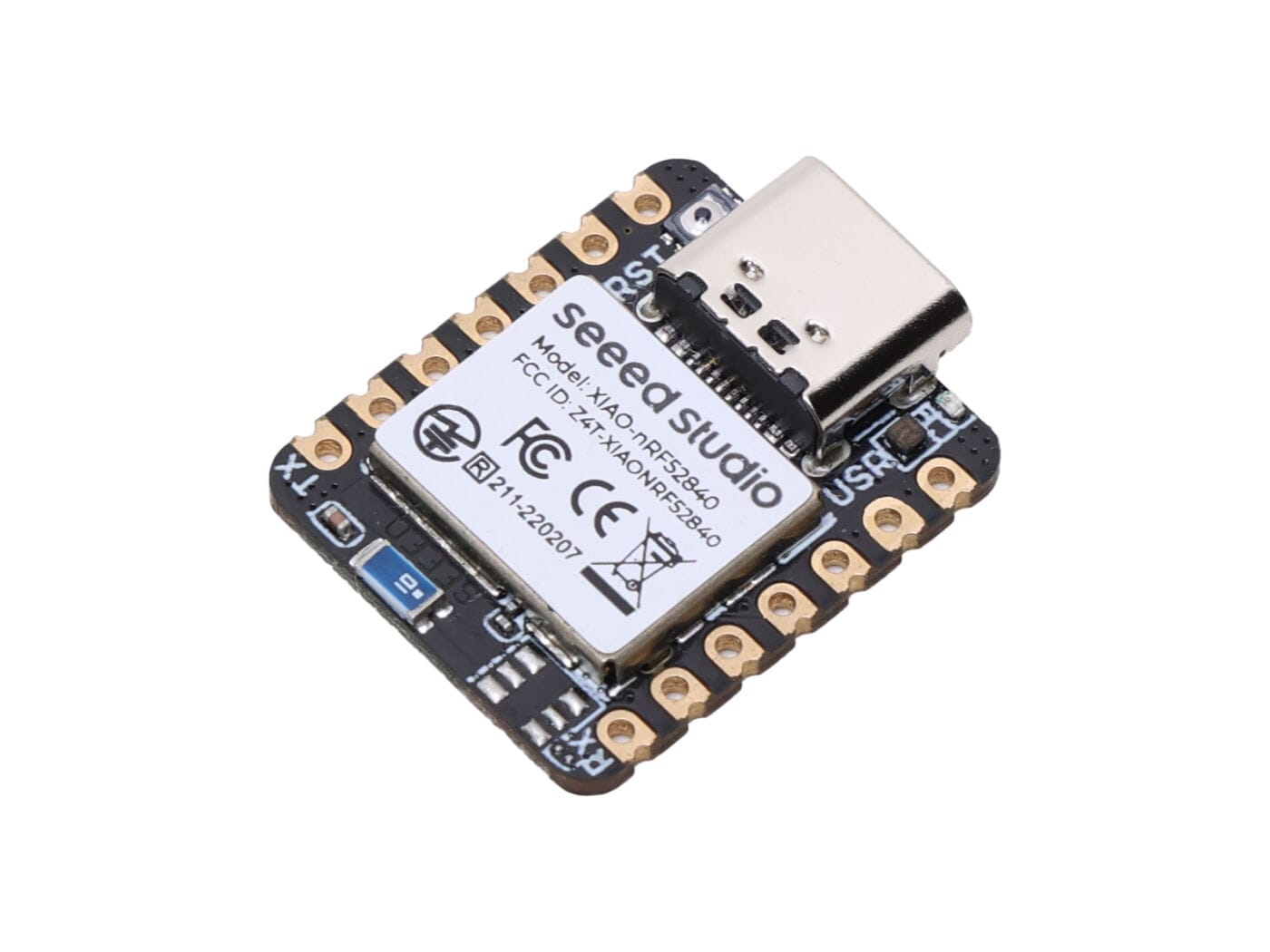
A much less morally dubious option is Seeed Studio's XIAO nRF52840. (Often referred to as the XIAO BLE.) This minuscule board can be found for about half the price of a Nice!Nano. Unfortunately it's downright austere when it comes to the pin count. It's a good option for keyboards with a low switch count, but you may need to bust out a shift register depending on your layout. Thankfully there are two NFC pins that you can repurpose for GPIO to eke out a bit more functionality.
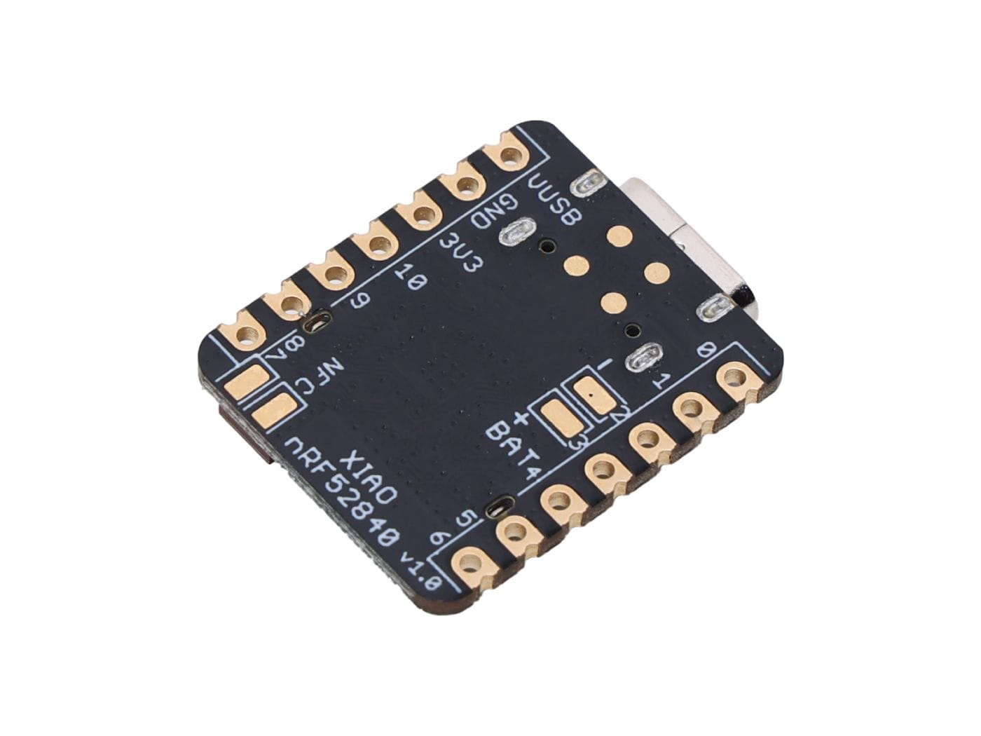
The XIAO is meant to be soldered flush to a keyboard PCB. It can be a little tricky for those new to soldering. Seeed decided to mount battery pins on the bottom of the XIAO nRF52840 in the center of the board. The only way of accessing these pins is to create some sort of connection underneath the microcontroller. The typical approach is to solder the microcontroller flush to the PCB and include a cutout so you can solder the power pins through the bottom of your PCB. There are also some approaches using standard microcontroller header pins in conjunction with spring-loaded pogo pins for the power connections on the bottom of the XIAO.
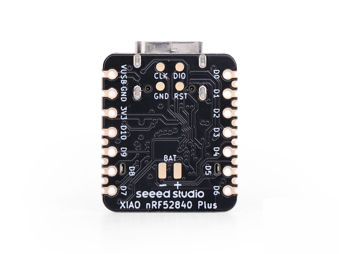
More recently Seeed Studio has also put out the XIAO nRF52840 Plus. This board adds nine additional pins to the existing XIAO form factor, at the expense of needing to deal with a much tighter soldering job. The power pins are also still on the bottom.
Wireless microcontroller options largely fall off after that. Whoever's creating the Supermini also recently cloned the XIAO nRF52840, but the legit board is already inexpensive enough that it's not worth straying from. The Nice!Nano is the easier option to work with, but the XIAO has helped empower some creatively small builds.
As for connecting the two halves, there's much fewer considerations here. After all: It's wireless! Just like QMK, ZMK will output a specific firmware file for your primary and secondary halves. The pairing between the primary half and the secondary half is baked into the firmware itself. When you power on the two halves near each other, they'll discover each other and silently connect without any input needed from the user.
That doesn't mean there aren't additional design considerations we need to consider for a wireless keyboard.
First and foremost, this is a wireless keyboard. It needs a battery to operate. Most DIY builders use a rechargeable LiPo battery that looks like a silver pillow with a yellow seam on one end. These batteries usually lead to a connector, but occasionally they'll just be sold with bare wires. Frustratingly, there's no industry standard for which orientation the battery is wired. Sometimes the power pin will be on the left, sometimes they'll be on the right. Just make sure you don't mix things up. If you want to be extra-careful, buy your batteries before you send your PCB off to get fabbed. Additionally, popular electronics vendor Adafruit sells LiPo batteries in a variety of sizes and shapes with consistent wiring.
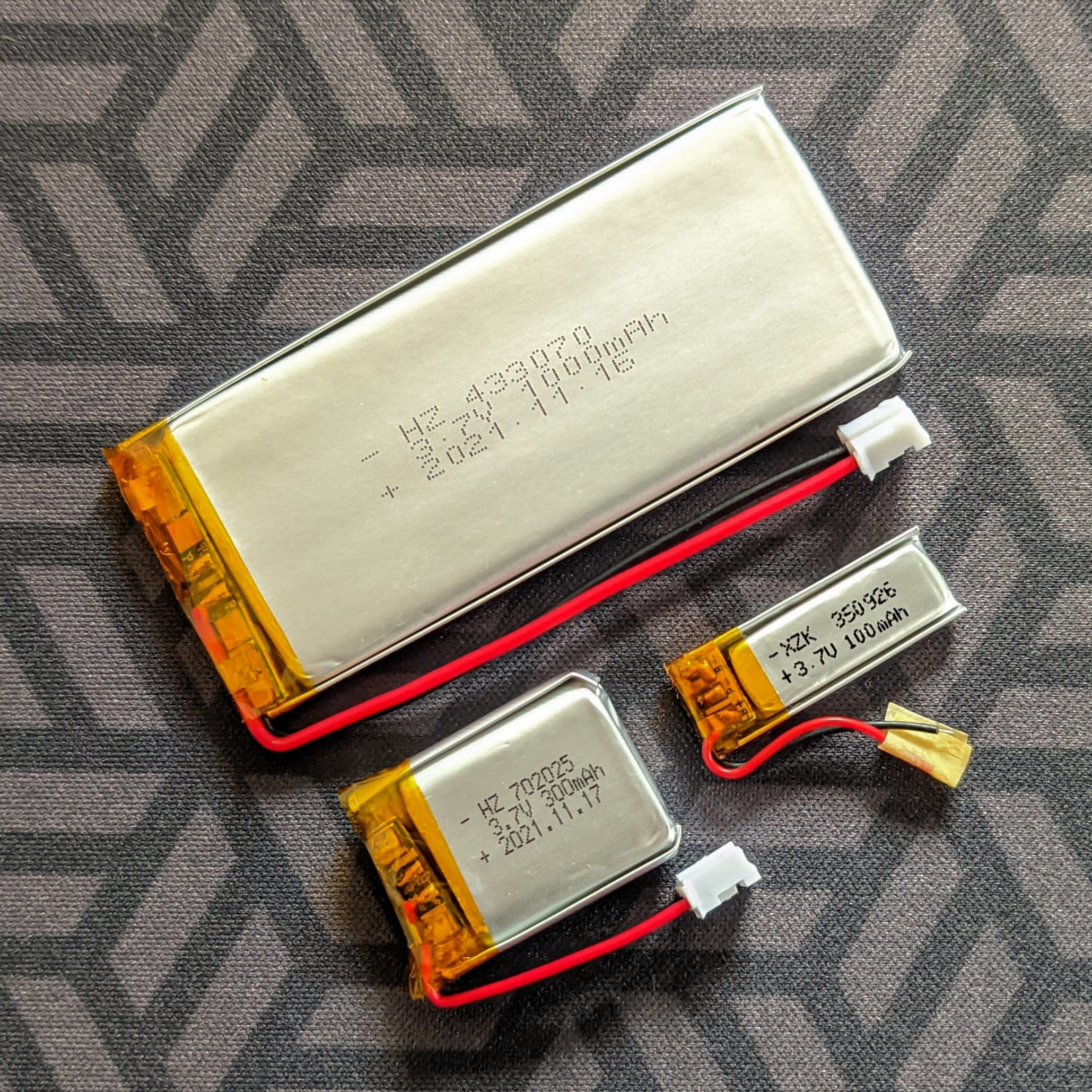
The keyboard building community has rallied around a generic 110 mAh battery. Its dimensions perfectly fill up the space underneath the Nice!Nano microcontroller when installed on a standard header socket. The primary half of your keyboard lasts for about a week with this battery, and the secondary will last for a few months. The half of your keyboard that does the communication with the computer unfortunately draws notably more power.
You can estimate other battery sizes on ZMK's power profiler web app. It can be tempting to place a huge battery underneath one’s keyboard, but just keep in mind LiPos really do not like being punctured. If your soldering has a habit of producing pointy bits, consider taking extra care to clean them up, or get creative with some electrical tape.
Shipping raw batteries often comes with additional logistics and limitations. The closer you can source your batteries the better. Sometimes that will just be a domestic electronics distributor with affordable ground shipping rates, or sometimes just Amazon. But it might be a good excuse to pick up at least a few parts from a keyboard specific vendor in your country.
Once you've got your battery picked out, you need some way of attaching it to your keyboard. If you're using a Nice!Nano you could directly solder the battery leads to the Bat+ and Bat- pins, but there are cleaner ways of going about things. The Bat+ pin is directly connected on the Nice!Nano to the RAW power pin, and Bat- is simply connected to the Nice!Nano's GND. We can leave the Bat+ and Bat- pins alone and simply wire things up to their equivalent on the standard Pro Micro header pins.
On the XIAO nRF52840, you do need to figure out how to get the positive lead from your battery connected to the Bat+ on the bottom of the XIAO. There is a Bat- on the bottom of the XIAO, but you can also connect the negative end of your battery to the normal GND pin.
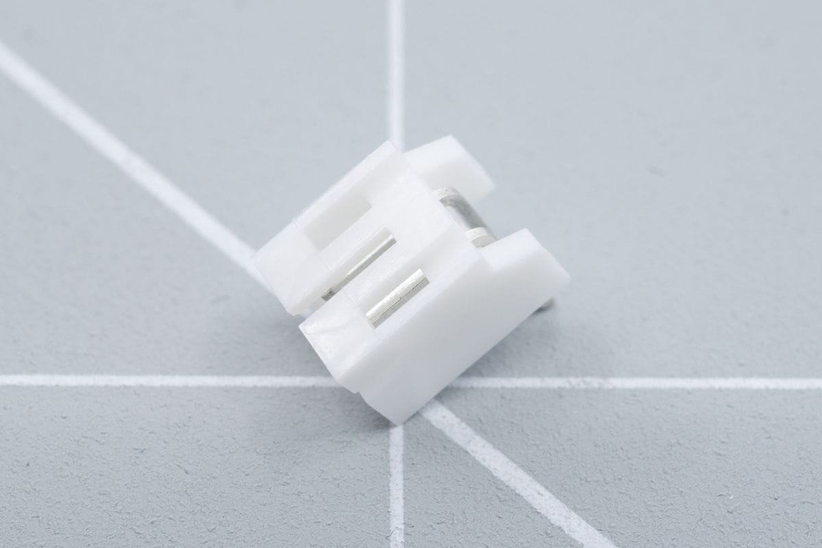
There's still the question of how to attach your battery. You can simply put a pair of through holes or SMD pads somewhere on your keyboard and solder the wires of the battery directly, but most of these batteries come with a "JST" connector. (Many connectors in the electronics world are just named after the company that popularized them. Thanks Japan Solderless Terminals!) JST sockets are easy to source, and they're available in beginner friendly through hole designs. It makes your battery a less permanent part of your keyboard, and allows you to replace it or move it to a new build more easily. Just remember to give your JST header a decent amount of room. Components can look spaced out on a PCB when viewing it in KiCAD, but you need enough room to physically insert the connector, and the wiring has to go somewhere as well.
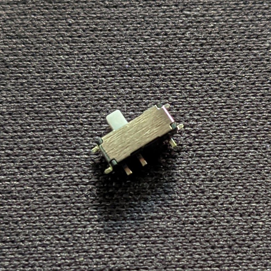
Wiring up the battery to the PCB also makes it easy to install a power switch. The Nice!Nano or XIAO BLE boot up the moment a battery is connected. We need some way of "disconnecting" the battery without actually having to physically unplug the JST connector every time.
Thankfully a simple slide switch can do the trick here. Keyboard part vendors and Ergogen's default footprints have coalesced around this small SMD switch, but you can use basically any switch you'd like.
The most common power switch is known as a "Single Pole, Double Throw" switch. Or an SPDT switch. "Single Pole" refers to there just being a single plastic arm controlling a single circuit. "Double Throw" indicates that there are two different connections the circuit can make. In practice, this just means a SPDT switch is a three pin switch that can make two different connections. When the switch is pushed to one side, it connects the pin on that side with the center pin. When you slide the switch to the other side, it connects the pin on that side with the center pin.
For our power switch, we're just going to use the center pin, and the pin in whichever direction we want to be the switch's "on" position. The third pin will be completely unused. We could technically get away with using a two pin "Single Pole, Single Throw" SPST switch, but SPDT switches are more common and can do a SPST's job just as well, so most part vendors will have a smaller selection of SPST switches.
Finally we need to figure out the circuit itself. To power the microcontroller, we need to connect the positive end of our battery to RAW/BAT+ and the negative end of the battery to GND. If either the battery's positive end or negative end are disconnected, the circuit will be incomplete and the microcontroller will shut off. This means we can put the power switch on either the battery's positive lead or negative lead. The switch will act like a temporary "cut" to the power when it's slid into the off position.
Both of these options work, but you usually want to fuss less with the positive end of the battery than the ground. So in a typical wiring you'll have:
- Battery’s Positive to the Microcontroller’s
RAW/Bat+ - Battery’s Negative to SPDT's Center Pin
- SPDT's Top or Bottom Pin to the Microcontroller’s
GND.
Setups will vary, so you could just as easily do:
- Battery’s Positive to SPDT's Center Pin
- SPDT's Top or Bottom Pin to the Microcontroller’s
RAW/Bat+ - Battery’s Negative to the Microcontroller's
GND.
About half my builds used the former method, and the other half used the latter technique. It mostly just comes down to what's easier to route.
That's it when it comes to wireless-specific considerations! You need an nRF52840 microcontroller, a battery, and a power switch. Just like the wired build, adding a small pushbutton for resetting your microcontroller is also recommended.
One quick note on something you typically don't need. Most of the common nRF52840 microcontrollers have battery charging circuitry built in. (The Nice!Nano, XIAO nRF52840, their Supermini clones, etc.) You don't need any fancy additional circuitry to charge and use a standard LiPo battery. If the battery's plugged in, it'll power the microcontroller. If you plug the microcontroller into USB the same time the LiPo battery's plugged in, it'll charge your battery. Simple as that. One tiny aside to this aside: This applies for those silver "pillow" like LiPo batteries. These LiPos have overcharge protection circuitry built into the battery itself underneath the yellow kapton tape. If you use an exotic battery like a rechargeable LIR2032 coin cell or 18650 barrel battery, you'll need to build in some of the battery protection circuitry yourself.
When in doubt, follow the best practices and prior art. No one wants a spicy pillow.
Why Not Both Wired & Wireless?

There are a variety of design philosophies when it comes to creating a keyboard PCB. For prebuilt kits, vendors will often create a flexible design with accommodations for both a wired split cable and wireless battery power management. These two approaches to building a split keyboard don't step on each other's toes from a hardware standpoint.
Unfortunately, it's a currently build time decision. You have to pick one or the other. A keyboard cannot dynamically flip back and forth between a wireless split keyboard and one joined together by a connecting cable.
ZMK has begun laying the ground work for wired split UART connections. Currently however you have to make the decision of what type of connection you're making when you flash your microcontroller. If you'd really like to be able to dynamically switch back and forth, go check their docs and see if there's been any changes. Currently everything’s pretty experimental. Based off their early work, it sounds like it will require specific hardware accommodations above and beyond QMK's current wired setups. Having a battery on both halves of your keyboards complicates things a bit.
Thankfully this limitation isn't a huge deal? As I touched on earlier, ZMK allows you to connect the primary side of your split keyboard with a USB cable. This allows you to use your ZMK keyboard like a standard USB keyboard. You can avoid flakey bluetooth, press F12 during a BIOS boot process, and generally treat it like a normal keyboard. It's just a little silly with the primary side being wired, but the secondary half still relying on a wireless connection.
There are some edge cases this might not cover. Some gamers may have latency concerns for the secondary side of their keyboard. You still need to keep the secondary half charged as well. The secondary half has significantly longer battery life than the primary half however, and you can charge and type at the same time.
Wireless builds are becoming popular enough that the vestigial wired connector footprint has started to disappear from some kits. The idea of flexibility is nice, but in this case, just focus on the use case you're most excited about.
What About 2.4 GHz Dongles?
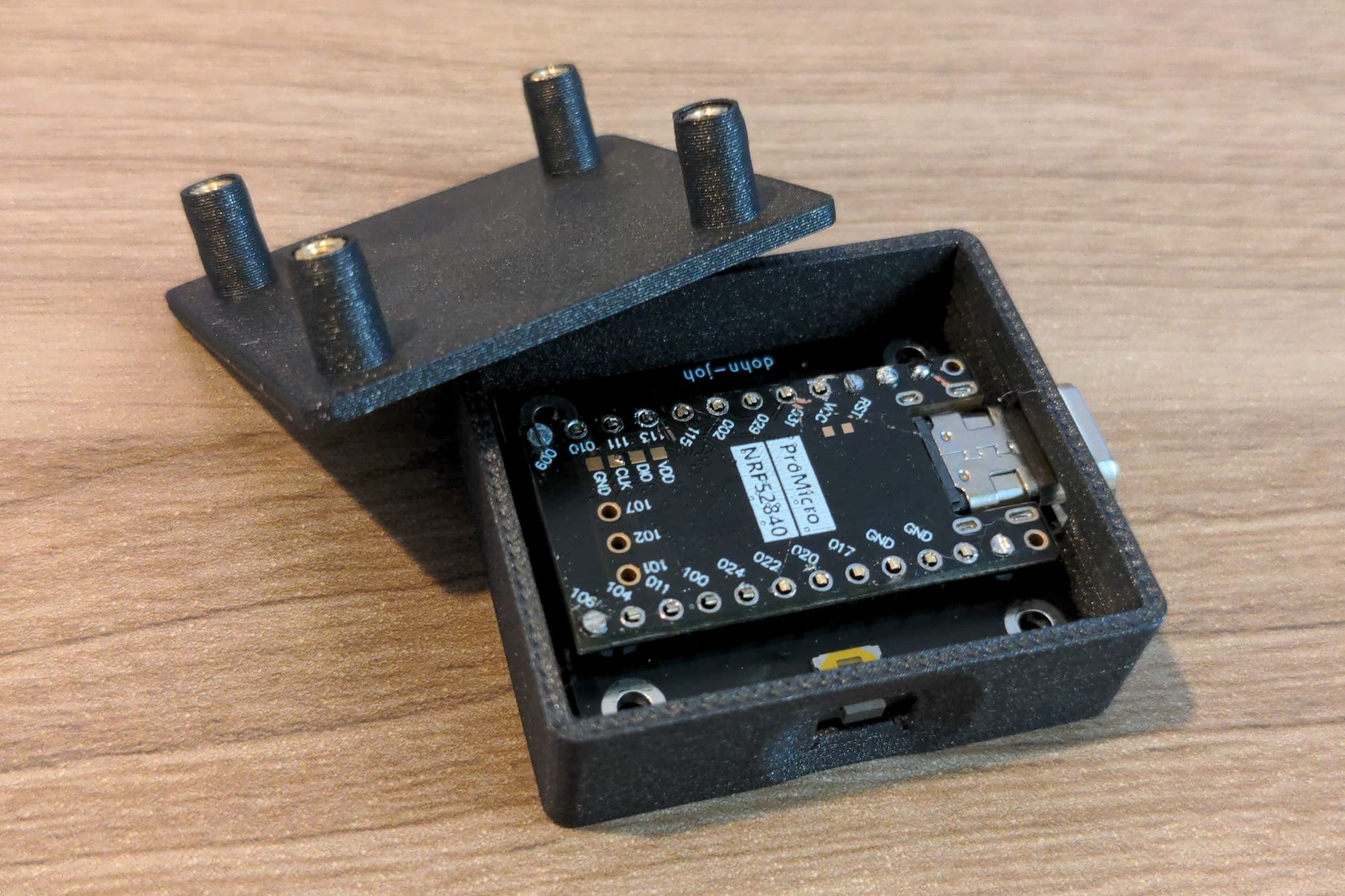
*Deep Inhale.*
Okay. Why do you want an RF dongle?
This ask is usually trying to get at something a bit deeper than just the protocol used to get the keystrokes to your computer. Logitech's Unifying Receiver dongles have been incredibly popular, and it's no surprise people are trying to recreate the experience with wireless setups.
To answer the question directly, there's not a great straightforward way of having a DIY wireless keyboard communicate over a non-Bluetooth 2.4 GHz RF signal. There are some options that may address the deeper question however.
If you're worried about Bluetooth latency, again, USB cables are an option. I might not be a ~pro gamer~ these days, but latency is not something you commonly see complained about when it comes to the nRF52840 and ZMK keyboards. The ZMK team is also continually looking into different options for improving latency. There's some promising work to be done in the future with Bluetooth connection subrating.
ZMK supports multiple Bluetooth hardware profiles. You can tap a layer key (a type of "Function" key) and 1 to pair with your desktop computer, and layer plus 2 in order to pair with your laptop. This helps with some device switching use cases, but it might not work in every situation where a USB dongle was useful. Some folks are still relying on physical KVM switches where the Logitech receivers come in handy.
There is an option for split ZMK keyboards known as "Keyboard Dongle" or "Dongle as Central". This allows you to introduce a third nRF52840 to your setup. This often bare component-free nRF52840 connects to your computer with a wired connection, and acts as the "primary" half of your keyboard. Both the left and right side of your split keyboard function as secondary "halves" of your keyboard.
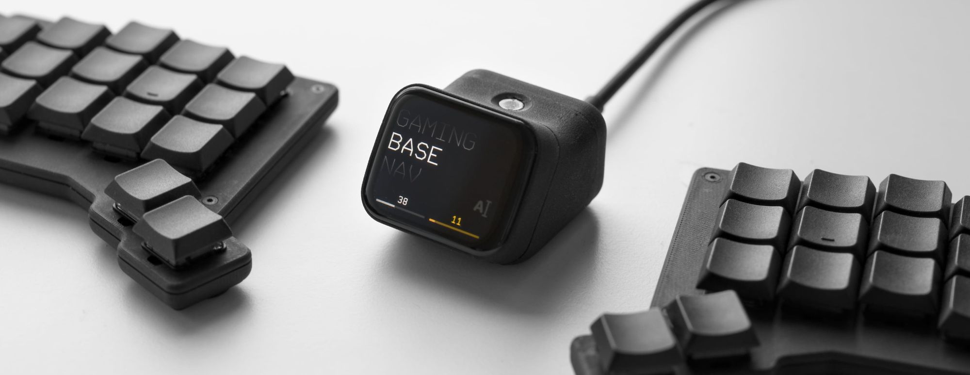
This was originally a bit of a wonky setup, but it's been gaining traction in recent years. There are a few vendors now selling ZMK dongles with LCD screens displaying a brief overview of the keyboard's state. You also benefit from the extended battery life of both halves of your keyboard operating as a secondary / peripheral split parts.
The big caveat is that you need to configure a ZMK keyboard for dongle mode when you flash the microcontroller's firmware. You can't hop back and forth between a traditional ZMK setup and ZMK's dongle mode. Dongle as central is great for a wireless keyboard which lives permanently at your desk, but it's less of a good fit for something you use at your desk and then toss into your bag while you're on the go.
If you do decide to build a keyboard dongle, it's worth noting that the XIAO nRF52840 is commonly sold in an affordable three-pack.
What about the ESP32?
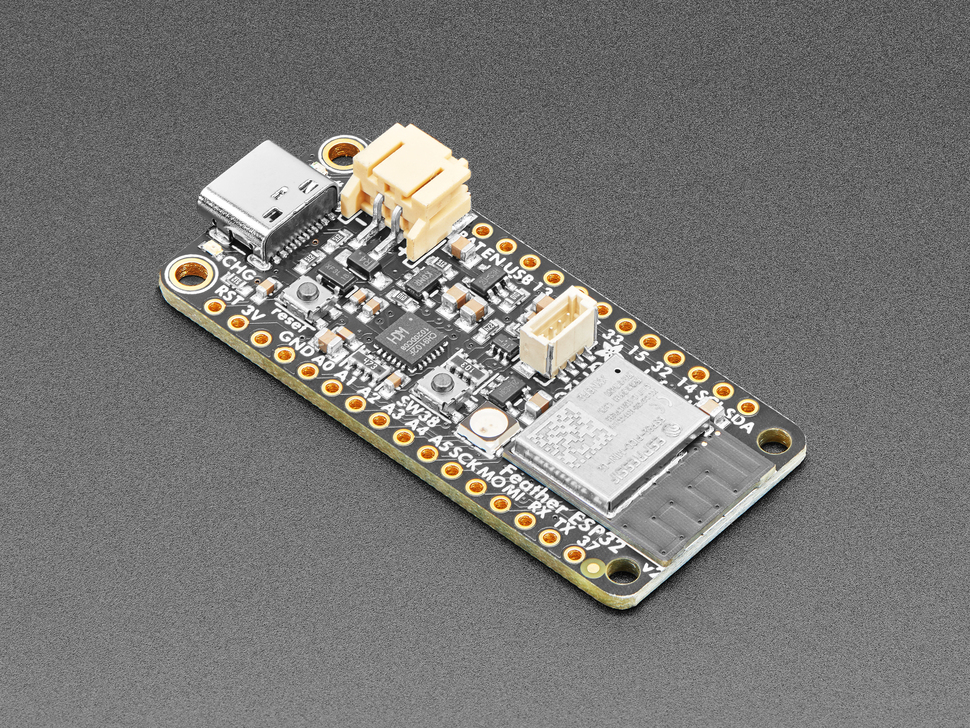
The capabilities of modern microcontrollers have expanded by leaps and bounds. Back in the early days of the Arduino, it was incredibly rare to see an affordable microcontroller which could handle Bluetooth connections. WiFi connections were completely unheard of. If you needed to get an Arduino talking to a networked device, you were buying an ethernet shield.
So to see the ESP32 burst onto the scene with Bluetooth, Wifi, and plenty of horsepower has made hobbyists' heads spin. It's just shy of being a low-end Raspberry Pi. This isn't a random edge-case power-user board either. Adafruit will sell you an ESP32 Feather for less than $20 USD. Naturally the question comes up, where are the ESP32 wireless keyboards?
The ESP32 isn't a great fit for keyboards for a few different reasons. It's a beefier chip, which means it has more of a power draw than the nRF52840. ZMK also lacks USB support with the ESP32, making it a bit trickier to deal with. That leaves you with the experimental parts of the KMK and RMK firmwares, or coding the device on your own.
As appealing as the chip may be, do yourself a favor and stick with the more trodden path. You'll be signing yourself up for an uphill battle if the first thing you do in your keyboard building journey is buy an ESP32 Feather.
Firmwares, Framing, & The Future

Open source projects are constantly evolving. I've had to update Let's Design A Keyboard with Ergogen several times over the last few years in response to updates made to Ergogen. Even this blog post needed revisions during the drafting process to reflect the changing state of keyboard firmwares.
The framing of "Wired Split Keyboard with QMK" and "Wireless Split Keyboards with ZMK" is somewhat reductive, and was mostly done to make the content digestible. Learning about Pro Micros and how the wired world does things makes the differences in the wireless space easier to pick up. In truth, QMK and ZMK are huge complex projects, and I was painting with a bit of a broad brush. QMK technically supports Bluetooth with additional hardware. (Although implementing this is exceedingly rare.) ZMK's first supported microcontroller was the wired STM32 chip. ZMK has supported wired unibody keyboards from the start, and has recently added support for split wired keyboards via a UART serial transport.
The current firmware meta may have changed if you're reading this article a while after it was published. ZMK continues to be a pleasure to work with, and its development team has been hard at work filling the gaps in the firmware's capabilities. The firmware's support for LEDs continues to improve, and there are already some early working examples of the dynamically shifting wired and wireless split transports. If you're designing a keyboard today with animated per-key RGB LEDs, it makes sense to build a wired RP2040 keyboard with QMK. If you're skipping the light show, there's already a strong argument to use ZMK for both wired RP2040 builds and wireless nRF52840 builds.
PCB Layouts: Symmetrical or Asymmetrical?
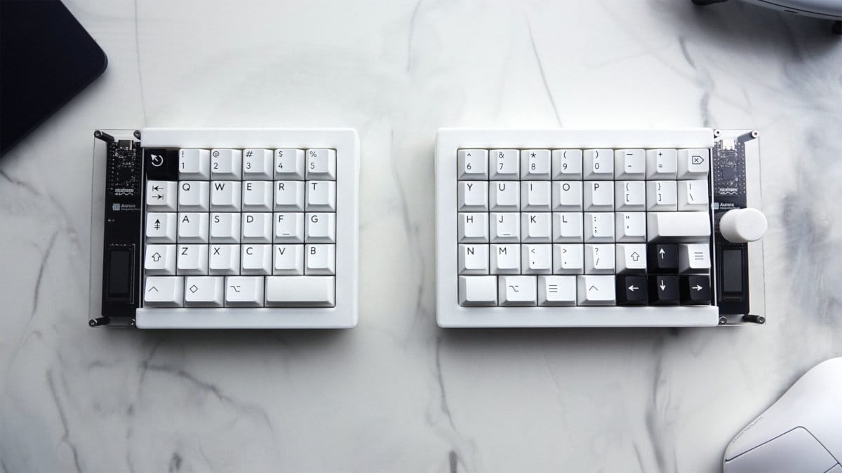
Alright! We've got the Wired vs. Wireless basics down. At this point you should have an idea of what sort of microcontroller you're going to use, and how that chip talks to other devices. Now we can get onto the PCB design bits of what was ostensibly supposed to be a PCB design guide.
The first question you need to ask about your split keyboard is whether or not the two halves are going to be mirrored copies of each other. If you know that one side of your keyboard is going to have 52 keys and the other half is only going to have 48 keys, you answer a lot of design questions right off the bat.
If the left and right side of your keyboard have two distinctly different shapes, you’re designing two PCBs. Simple as that. The end result of your designing will be two KiCAD files that you export and send off to your PCB fab. Handling this in Ergogen is pretty straightforward: You create two project folders and two Ergogen configs. You end up with mykeyboard-left and mykeyboard-right. If you're using the web view, make sure you save two different config files on your local computer so you don't accidentally overwrite something when you switch between the left and right halves. I haven't personally created distinct asymmetrical Ergogen files before, so I unfortunately don't have any go-to tips on mirroring your points for the right half. There will be some extra effort involved.
You may have seen some PCB designs online that use small breakaway tabs to connect two PCBs together. While you can technically design your split keyboard in a single KiCAD design file, PCB fabs usually have pretty strict policies around customers doing their own "panelization". Fab prices are largely based off the amount of PCB material you use, not the number of designs you upload. So panelizing your designs yourself generally doesn't save you a substantial amount of money. If you're still interested in exploring more about these breakaway tabs, Sparkfun has a good white paper discussing the best practices of these affectionately named “Mouse Bites”.
The downside of designing a distinct left and right half is that you need to fab two different PCBs. PCB manufacturers have order limits requiring you to purchase 3-5 copies of each design that you upload. So split designs with a distinct left and right half often end up mailing you a whopping 10 PCBs.
There’s got to be a better way, right? Well, if your split keyboard has a mirrored symmetrical design, there just might be. Welcome to the complex topic at the heart of this guide.
Reversible PCBs
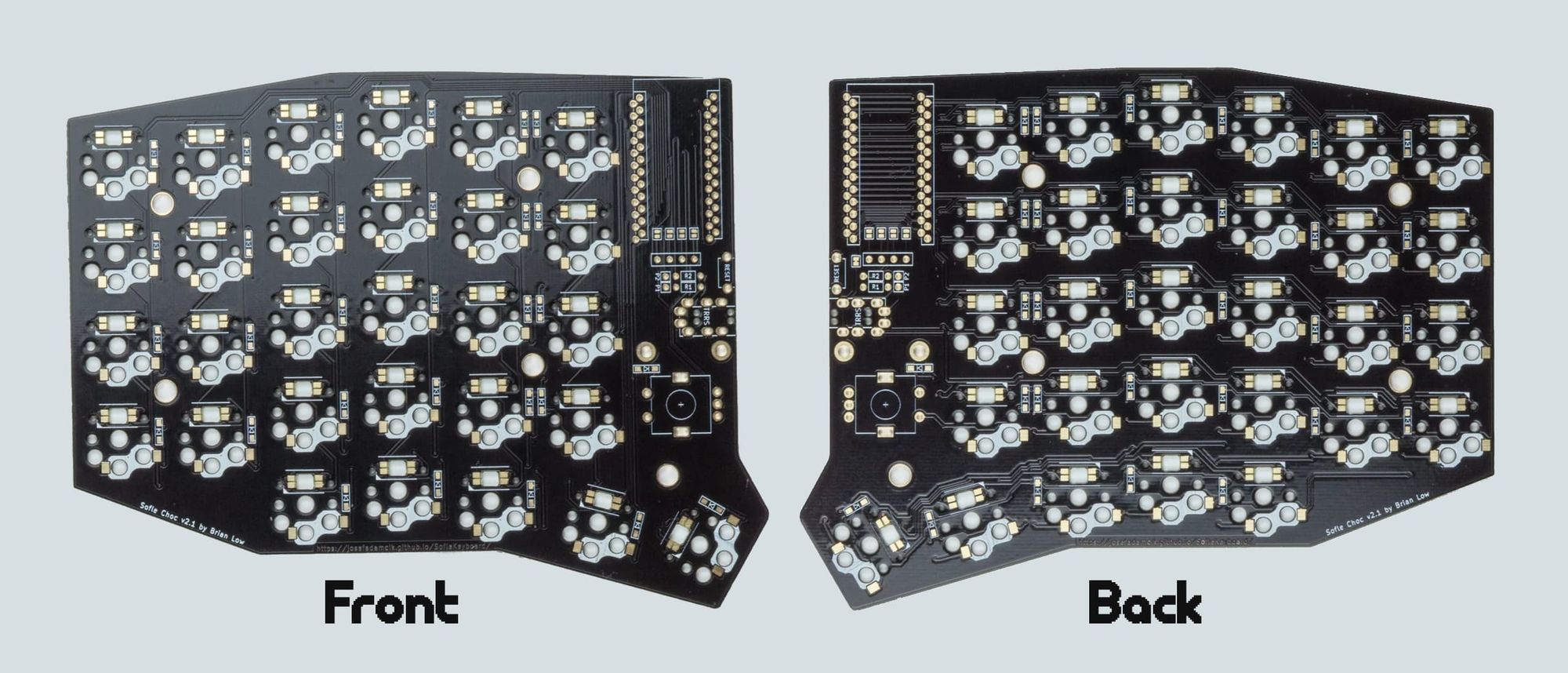
The vast majority of split keyboards aren't asymmetrical curiosities. Most of the time both halves have an identical (mirrored) layout on the left and right halves, with nearly the same hardware on each side. Occasionally footprints for components such as rotary encoders or LCD screens will only be populated on one side of the keyboard, but the overall shape of the PCBs and the layout of the switches is identical.
For these symmetrical split keyboards, you can still go with the dedicated keyboard-left and keyboard-right Ergogen project approach. This can be handy for things like custom left and right PCB art, or accommodating atypical hardware only on one half of the keyboard like trackpads. In a world where PCB fabs force you to manufacture 5 copies of any design you upload however, it would be ideal if we could somehow use the same PCB design for both the left and right halves of our split keyboard.
The issue is that the left and the right halves aren't technically identical. They're mirrored. The left half of your keyboard has a nice little arc for your thumb on the right side. You want that arc to be on the left side of your right half. Even with squared off ortholinear keyboards, people tend to prefer mirrored microcontroller placements.
Thankfully, PCBs are fairly versatile, and designers are a crafty bunch. To "mirror" a physical PCB, all you need to do is literally flip it over. Your standard 2-layer PCB allows you to solder components to the front or the back. Typically this would just be a diode on the front and a resistor on the back, but no one says you can't solder a keyboard switch to the "bottom" of a PCB.
Simply put, reversible PCBs are keyboard circuit boards which have been designed to function regardless of whether a component is soldered to the front or to the back. But how exactly is this accomplished? It depends a bit on the part you're trying to accommodate. Some are straightforward, and some require a bit more creativity.
Reversible Footprint Basics
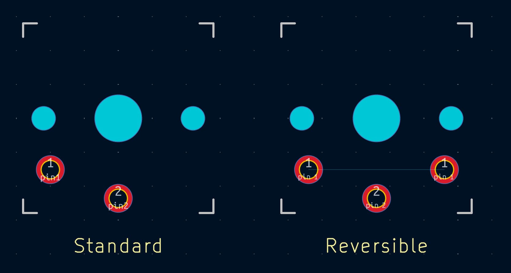
If you've poked around Ergogen a bit, you may notice that some footprints have a reversible: flag you can set. Some components work on the front or back side of a PCB without any tweaks, but the majority of the parts on your keyboard will need at least a bit of accommodation.
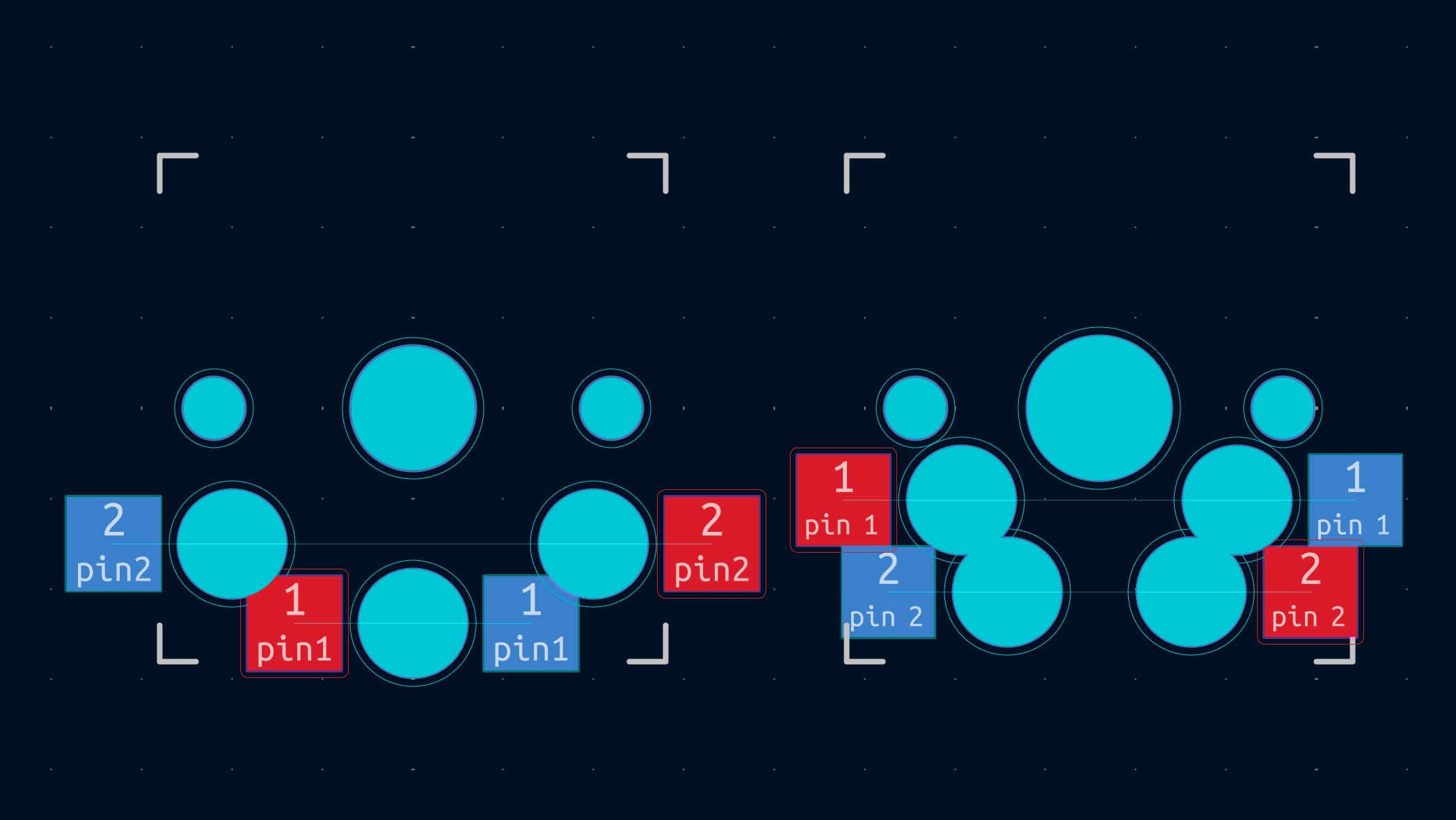
Let's look at a Choc switch for example. (This applies to MX switches too, so don't skip over this part if you're planning on making a reversible MX build.) The Choc v1 switch has 5 elements to it: Three plastic posts, a center pin, and a pin that's offset on the right side of the switch. (That is to say, the right side of the switch as you insert it into the PCB.)
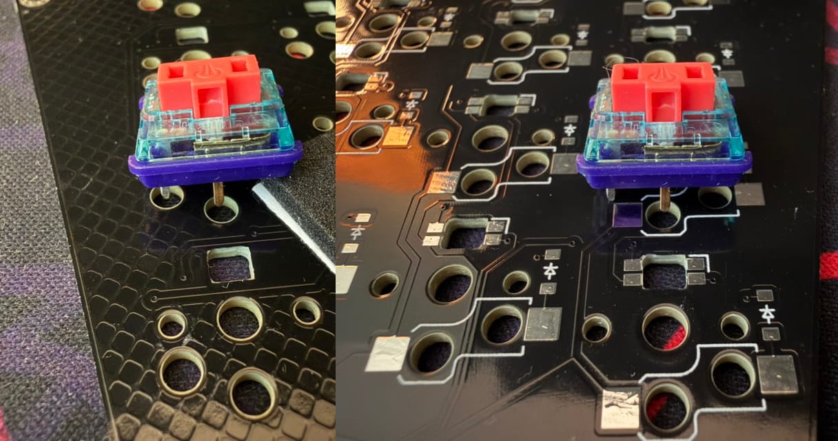
Inserting the switch into the standard footprint on the front of the PCB works fine. If we flip the PCB over however, we end up mirroring the standard footprint. The symmetrical aspects of the footprint are fine. The center plastic post, the two posts on the left and right, and the center pin all line up fine with our switch. In our mirrored footprint however, the second pin is now offset on the left. If we try to insert the Choc v1 switch on the bottom of the PCB, the pin on the right has nowhere to go and just runs into PCB material.
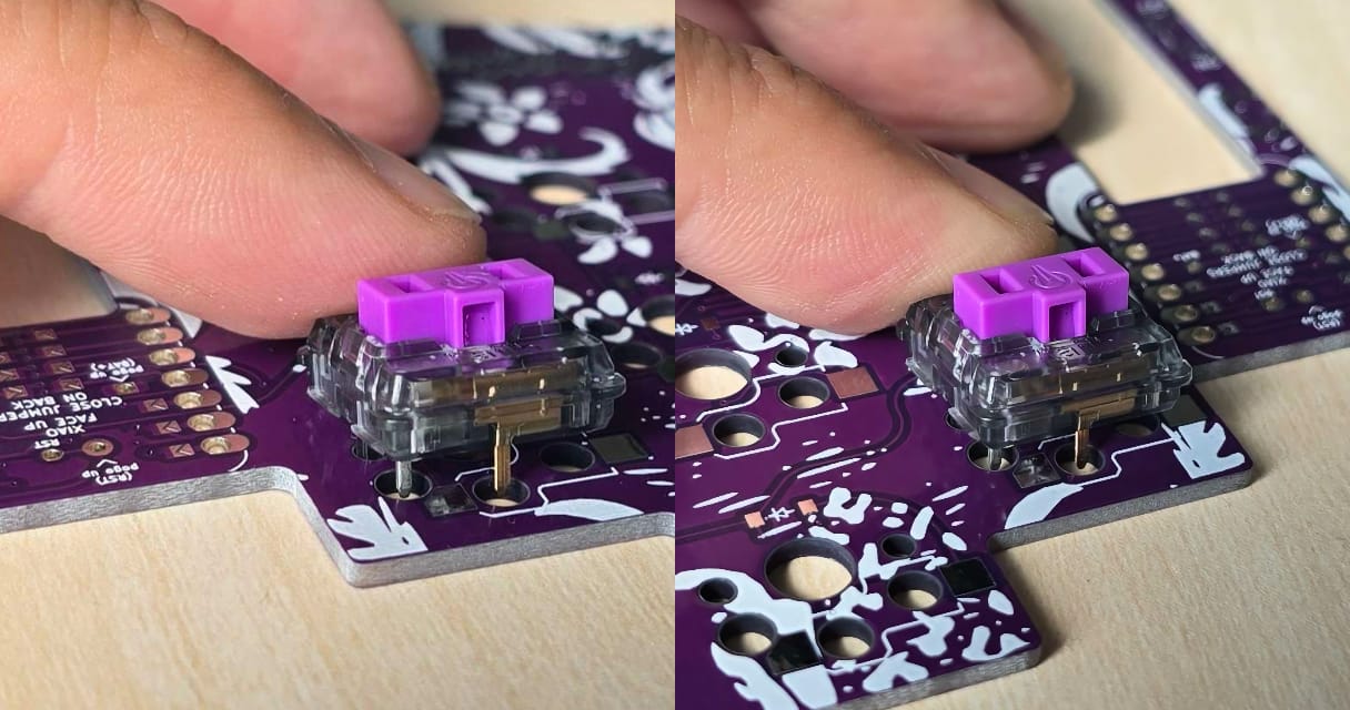
Fixing this in a Choc switch footprint is pretty straightforward: We add an extra through hole for the second pin. By putting a pin offset to the left and right, we can physically insert the Choc switch on the front or back of the keyboard.
When it comes to wiring this footprint up, we simply need to define the left and right through holes to connect to the same part of our keyboard wiring. As you can see in the screenshot, the center through hole is "Pin 2" in the wiring, but the left and right through holes are both considered "Pin 1".
When you insert the switch on the front, you'll use the right version of Pin 1. When you insert the switch on the back, you'll use the left version of Pin 1. Since they're both going to be connected to the same part of the circuit, and only one orientation of the switch will be inserted at a given time, keyboard will continue to behave as normal.
Accommodating physically asymmetrical parts is half the job of reversible footprints. The other portion comes from dealing with electrically asymmetrical parts.
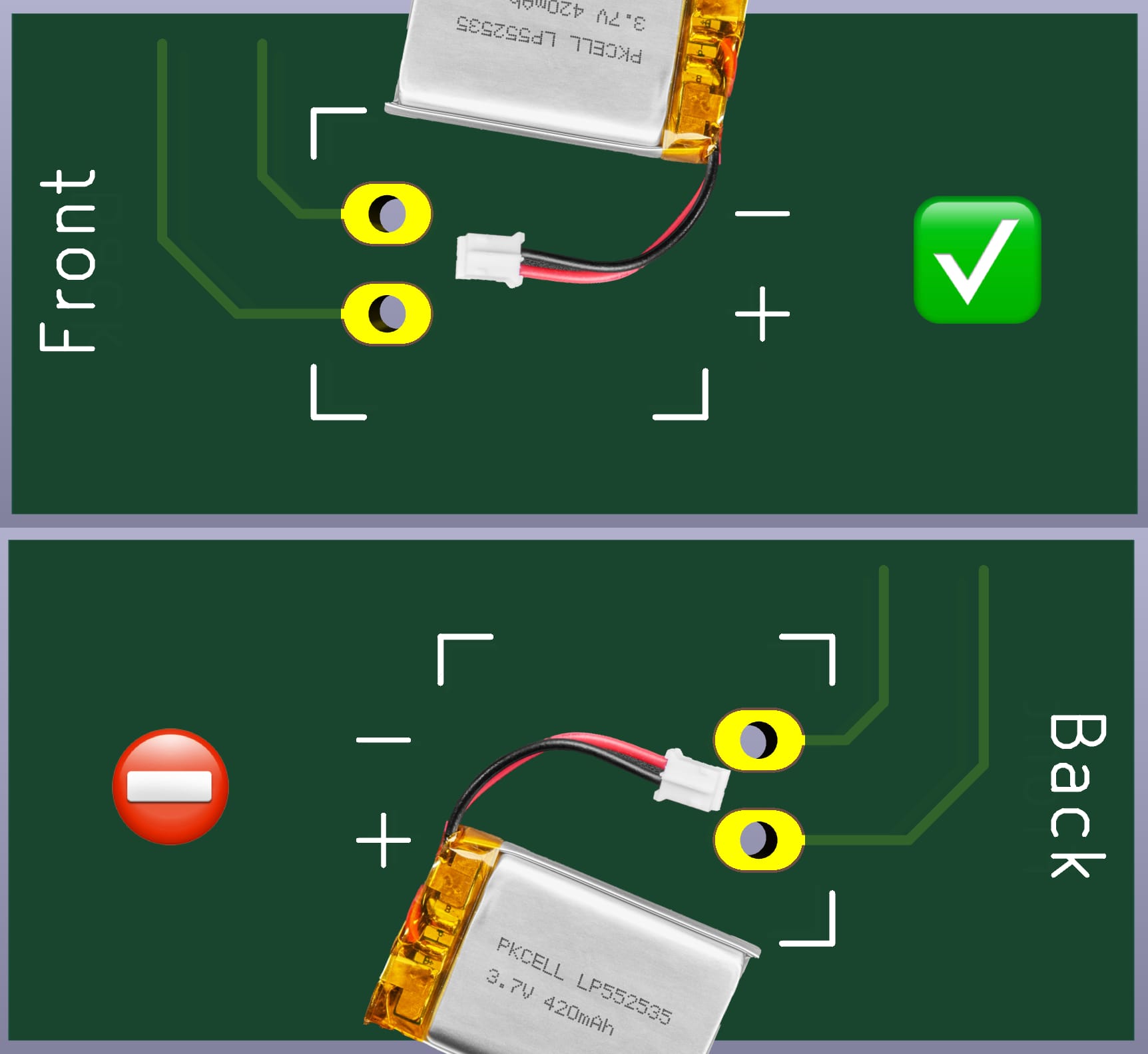
A Choc switch is a pretty simple component. You press the key down and Pin 1 is connected to Pin 2. The wiring doesn't matter as long as those two pins are being bridged. But what about something where the wiring is very important. You don't want to mix up Bat+ and Bat- on your LiPo battery header after all, right?
The LiPo battery JST footprint is pretty simple. It's just a pair of through holes. We don't need to do any special accommodation to make the part physically fit when we insert the header on the front of the PCB or the back. But something odd happens when we insert the JST header on the back side of the PCB: Its wiring gets flipped.
Often the Bat+ pin is on the right of the header, and the Bat- pin is on the left of the header. (Again, there's no industry standard for this. Check the wiring of your battery before you insert it into a keyboard.) But if you insert the JST header into the back of your PCB, suddenly Bat- is on the right of the header, and Bat+ is on the left.
This is where the real crux of reversible PCBs comes into play. We need to devise a way of mirroring footprints without mirroring critical wiring. The problem is that we're just dealing with one PCB design. We can’t magically change the wiring when we flip the PCB over. The final wiring needs to be addressed somehow as we go to solder the front or back component into place.
There’s no “correct” way of making a reversible footprint. There are different conventions and schools of thought. This JST header is a good example to demonstrate two of them.
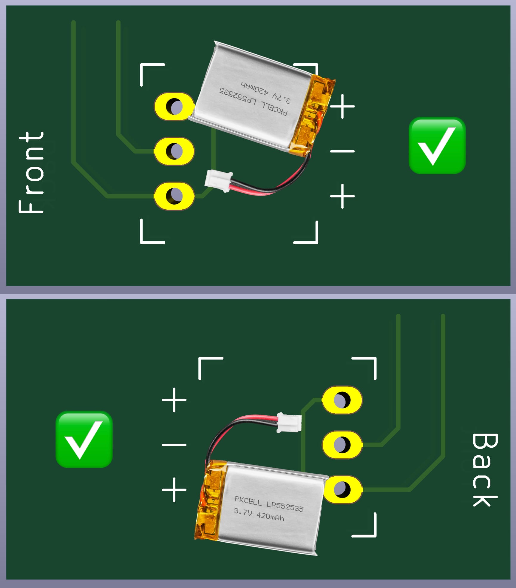
Much like the Choc footprint, we can get ourselves out of trouble by adding additional pins. Instead of just having a pair of Bat+ and Bat- pins, we can create through holes to Bat+, Bat-, and Bat+ again.
This solves our dilemma in a pretty straightforward manner. When soldering the header into place on the front side, we use the second and third pins to get Bat+ on the right, and Bat- on the left. When we flip the board over, we use the first two pins. This keeps the Bat+ and Bat- orientation the same across both halves of our keyboard.
It also moves the JST header up about a millimeter on our secondary half. If you’re a stickler for symmetry, you might be looking for a cleaner solution. Thankfully we have options there too.
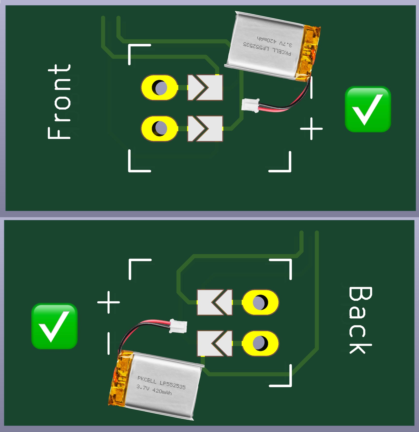
PCBs have a concept known as a “jumper pad”. It’s two pieces of exposed metal which are typically not touching, but can be bridged together with some solder to create a new connection in a circuit. These are used all over the place in modern reversible PCB designs. The idea is that you don’t wire the footprint directly into your microcontroller immediately. Instead, your part gets routed to two sets of jumper pads first.
One set of pads will be soldered for connecting the “Standard” orientation of the part, and the other set of pads will be soldered shut for the “Reverse” orientation of the part. Only one set of pads is soldered at a time.
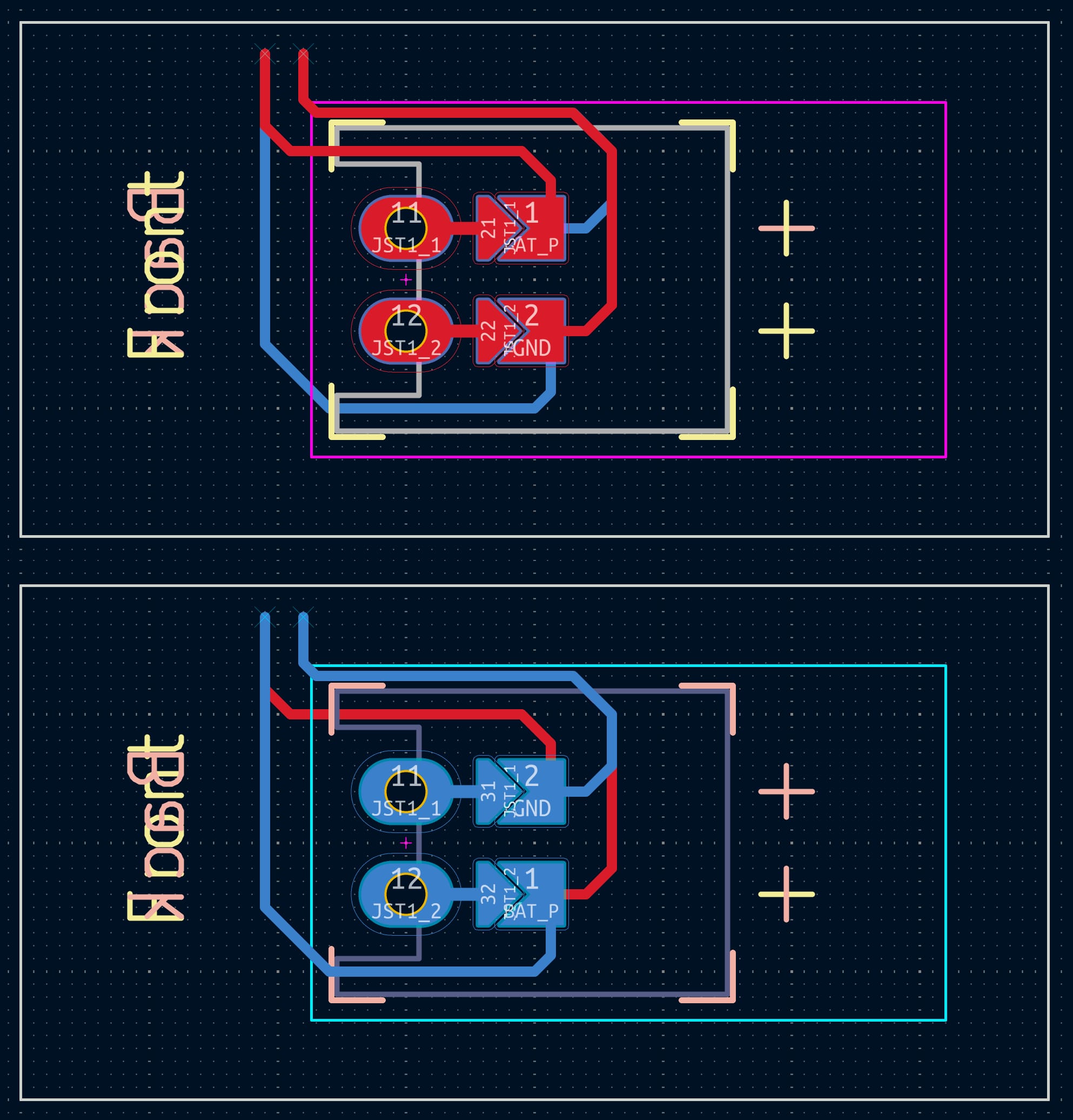
Jumper pad configurations vary, so make sure you read the documentation of the footprint you're using. A common convention is to require builders to solder the jumper pads on the opposite side of the component they're soldering onto the PCB. This allows you to still access the pads for troubleshooting purposes, but it's not a universal convention.
In this case, when we put the JST header on the front of the PCB, we'd want to solder the pads on the back. When we put the JST header on the back of the PCB, we want to solder the jumper pads on the front. This way BAT+ and GND signals always make their way to the right pin.
This two pin example carries across to larger components as well. If you had a six pin component, you’d have twelve jumper pads total. Six pads would give the standard wiring, and the other six reverse pads would swap things as needed. You might get the signal for Pin 1 swapped with Pin 2, Pin 3 swapped with Pin 4, Pin 5 swapped with Pin 6, etc.
This all takes a little bit to wrap your head around. Sketching a footprint onto the front and back of a physical post-it note and flipping it around in your hands can help visualize things for you. KiCAD’s 3D PCB preview is useful too.
Thankfully not every component will need an excess of jumper pads. Most keyboard firmwares allow you to remap pins for your primary and secondary halves. You might have a rotary encoder plugged into Pin 1, Pin 2, and Pin 3 on your primary half, but Pin 14, Pin 15, and Pin 16 on your secondary half, etc. Jumper pads are primarily useful for moving around signals which can’t be remapped in software such as power lines or ground pins.
If you're getting overwhelmed by all these reversible concepts, it's worth emphasizing that you can always just make a dedicated PCB design for your left and right halves. There are plenty of people who don't find it worth all the added complexity to deal with reversible footprints, or like the freedom of being able to have slightly different component placements and silkscreens on their two different halves. There is a cost impact, but PCBs are typically not the most expensive element of a keyboard's cost. Skipping the reversible steps covered in the rest of this guide will cost you about $15 USD in additional PCB manufacturing and shipping fees.
Ergogen & Reversible PCBs
meta:
  engine: 4.1.0
units:
  # Web View Resizing
  $default_width: cx
  $default_height: cy
  # Proxy Spacing Variables
  kx: cx
  ky: cy
  # Padding Variables
  px: kx + 4
  py: ky + 4
points:
  zones:
    # The primary 6x4 key matrix, plus 3 modifiers.
    matrix:
      # Position in center of KiCAD workspace.
      anchor:
        shift: [100, -100]
      # Choc spacing
      key:
        padding: 1ky
        spread: 1kx
      columns:
        # Hide the first two mods and the last mod.
        # Provide a Sofle-like column stagger.
        outer:
          rows.mod.skip: true
          key.column_net: col1
        pinky:
          rows.mod.skip: true
          key.column_net: col2
        ring:
          key:
            stagger: 5
            column_net: col3
          rows.mod.column_net: col1
        middle:
          key:
            stagger: 2.5
            column_net: col4
          rows.mod.column_net: col2
        index:
          key:
            stagger: -2.5
            column_net: col5
          rows.mod.column_net: col3
        inner:
          rows.mod.skip: true
          key:
            stagger: -2.5
            column_net: col6
      rows:
        # Four main rows, one partial row.
        mod:
          row_net: row1
        bottom:
          row_net: row2
        home:
          row_net: row3
        top:
          row_net: row4
        num:
          row_net: row5
    # Thumb cluster for Layer and Space keys.
    thumbs:
      # Choc spacing
      key:
        padding: 1ky
        spread: 1kx
      # Place thumbs where the inner mod would go.
      anchor:
        ref: matrix_inner_mod
        shift: [2, -2]
      columns:
        # Fan thumbs out by -15 degrees.
        layer:
          key:
            splay: -15
            column_net: col4
        # Spacebar uses a 1.5 wide key.
        space:
          key:
            width: 1.5kx
            splay: 75
            shift: [2.5,-3.25]
            column_net: col5
      rows:
        # Thumbs only have one row.
        cluster:
          row_net: row1
outlines:
  keys:
    - what: rectangle
      where: true
      size: [kx-0.5,ky-0.5]
  board:
    - what: polygon
      operation: stack
      points:
        - ref: matrix_outer_num
          shift: [-0.5px,0.5py]
        - ref: matrix_ring_num
          shift: [-0.5px,0.5py]
        - ref: matrix_middle_num
          shift: [-0.5px,0.5py]
        - ref: matrix_middle_num
          shift: [0.5px,0.5py]
        - ref: matrix_inner_num
          shift: [0.5px,0.5py]
        - ref: matrix_inner_num
          shift: [0.5px+27,0.5py] # Eyeballed +27 to give room for the microcontroller.
        - ref: thumbs_space_cluster
          shift: [0.5px,-0.5py]
        - ref: thumbs_space_cluster
          shift: [-0.625px,-0.5py] # This technically probably should have been 0.75 for a 1.5u switch, but it looked a little weird.
        - ref: thumbs_layer_cluster
          shift: [0.5px,-0.5py]
        - ref: thumbs_layer_cluster
          shift: [-0.5px,-0.5py]
        - ref: matrix_ring_mod
          shift: [-0.5px,-0.5py]
        - ref: matrix_outer_bottom
          shift: [-0.5px,-0.5py]
  preview:
    - name: board
    - operation: subtract
      name: keys
pcbs:
  tutorial:
    outlines:
      main:
        outline: board
    template: kicad8 # Include KiCAD 8 template to use ceoloide footprints.
    footprints:
      [...]
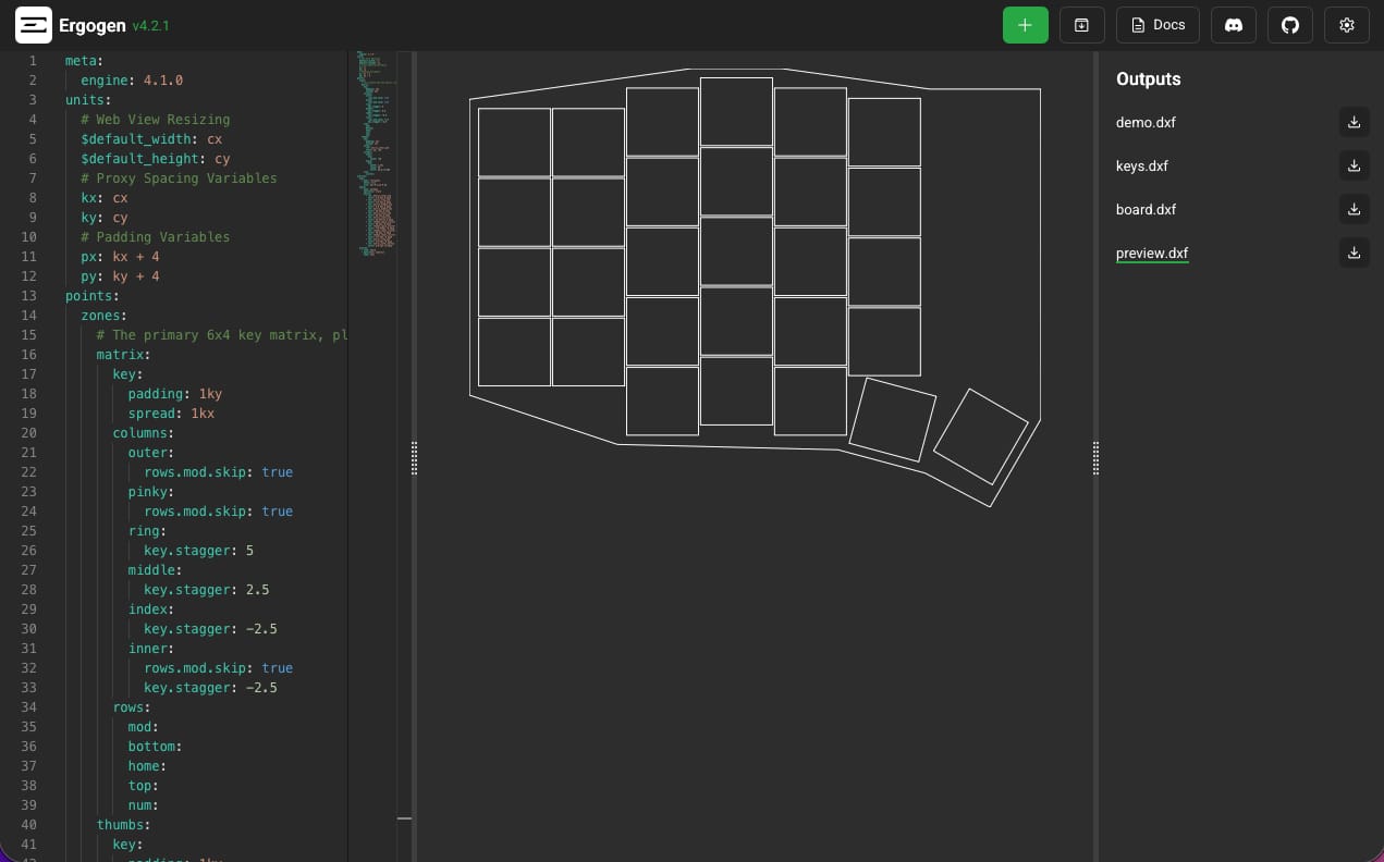
Ergogen doesn't have an explicit "Reversible" mode or configuration setting. You simply define a single side of a split keyboard and make accommodations in the PCB footprints section to account for the fact that you're going to be flipping the PCB over for the other half of the split keyboard.
So to get us started off, let's quickly define a six row, five column layout. This is heavily based off of the original Let's Design a Keyboard with Ergogen design. If you'd like a more thorough explanation of the points: and outlines: section, go check out that guide. The big difference with this split design is that we no longer have a mirror: section repeating the left half of the keyboard onto the right.
Again, Ergogen is very much a land of conventions and community habits. Most designers use the left side of a keyboard as their "Primary" side. You could technically define the right side if you wanted.
The board outline is similar to the original Let's Design A Keyboard with Ergogen technique. It defines a polygon which traces around the outside edge of the keyboard. The shift properties move the edge of our polygon to the corners of one of the switches. I just eyeballed the top right corner to give an additional 27mm for the microcontroller.
Now that we've got the points: and the outlines: defined, we can begin defining the pcbs: section. This is where the majority of the reversible work happens.
Reversible Ergogen Footprint Libraries

Back in Part 4 of Let’s Design a Keyboard with Ergogen, I explained how to add non-standard external footprints to an Ergogen config. This section of the guide is still valid, but we have a few more options than diving headfirst into Ergogen on the command line.
Community member ceoloide has done an amazing job improving the web version of Ergogen. Ergogen.xyz now supports users uploading custom footprint files. In addition to this, you can now point the Ergogen web view at a GitHub repository and automatically pull in the config and its associated footprints.
Taking things one step further, ceoloide has also created a community footprint repository full of common keyboard building components. This library is included by default in the web view. In the what: property in your PCB section, simply include the ceoloide folder name in front of the part name such as what: ceoloide/footprint_name to call one of the community footprints.
The footprints in this library have a dizzying number of custom params: one can set. Most of them include a reversible: true/false option where it makes sense. I’ll be calling out these footprints where they’re applicable.
The stock footprints built into Ergogen are also still handy. Many of these also contain reversible: params you can take advantage of without needing to use an external library.
If you can’t find a reversible footprint for a particular component, you can always make your own. The full process is outside of the scope of this guide, but Genteure's KiCAD2Ergogen is a great converter to automatically turn a standard KiCAD footprint into an Ergogen footprint. It’s a good starting place when looking to make your own Ergogen footprints.
One last bit before we dive into the individual parts: Ergogen v4 originally targeted KiCAD 5's file format when outputting PCBs. KiCAD is backwards compatible, so the modern KiCAD 10 (or whichever version it is at now) can open Ergogen v4 outputs without any issues. KiCAD will give you a small warning about the old file and how it will be updated if you save anything.
KiCAD files themselves won't give you any issues, but there's a chance you may get tripped up on KiCAD footprints. KiCAD made several breaking changes to footprint definitions since KiCAD 5. (Particularly with how curved arcs are handled.) Most KiCAD footprints you find online will be targeting the more modern KiCAD footprint spec, and KiCAD will throw an error if you try to use a converted KiCAD 10 footprint inside of the old KiCAD 5 file type Ergogen outputs.
To solve for this, the PCB section of an Ergogen config can include a template: kicad8 parameter to indicate that it’s using the more modern KiCAD 8+ spec for the footprints you’re adding. This includes all of ceoloide's community footprints. Don’t forget to add this parameter at the start of your PCB section if you plan on using his library.
Reversible Footprint Overview
Here’s a non-exhaustive list of common keyboard footprints and how they’re adapted to work in reversible PCBs. These are presented in no particular order, other than trying to make the concepts digestible.
Mounting Holes
mounting_hole:
  what: ceoloide/mounting_hole_plated
  where: mountingholepoint
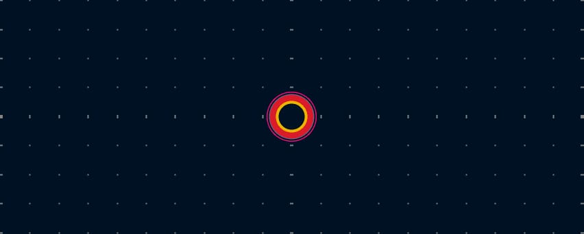
When building a PCB, it’s always important to think about how you’re going to mount a case. If you’re going to use one of course. Ceoloide’s mounting_hole_plated footprint are nice handy ways of adding M2 screw holes to a PCB they’re small enough to include in the space between two Choc switches.
I’m mostly including these in the list to show that not everything is going to have a reversible: param. You’ll start getting compile errors if you just add them willy nilly to every part in your PCB list.
Reset Buttons

reset_front:
  what: button
  where: resetbuttonpoint
  params:
    side: F
    from: RST
    to: GND
reset_back:
  what: button
  where: resetbuttonpoint
  params:
    side: B
    from: RST
    to: GND
One last, “Why is this even here?” entry to kick things off! Push buttons are two or four pin buttons with the simple job of connecting two wires together. (The 4 pin models have redundant pins to make them more structurally sound, but work the same way.) Since reset push buttons just need to connect RST and GND, the switches don’t need to be mounted in a particular orientation, and there’s nothing we need to compensate for when mirroring the footprint.
It’s important to remember that not every component will need an explicitly reversible footprint. If you're using the built-in Ergogen footprint, you can simply just place it twice. Once on the front, once on the back.

reset:
  what: ceoloide/reset_switch_tht_top
  where: true
  params:
    reversible: true
    from: GND
    to: RST
If you would like to dip into ceoloide's library, he does offer a few more push button styles. These do come with a reversibility option to save you the step of defining the second footprint. I'm quite partial to these small two pin through hole pushbuttons.
Diodes

diode:
  what: diode
  where: true
  params:
    from: "{{colrow}}" # Intersecting column-row net connecting to the switch. (Don't swap with 'to'.)
    to: "{{row_net}}" #  Row net connecting to Microcontroller. (Don't swap with 'from'.)
diode:
  what: ceoloide/diode_tht_sod123
  where: true
  params:
    reversible: true # Includes SMD pads on both sides of the PCB.
      include_tht: false # SMD only.
    from: "{{colrow}}" # Intersecting column-row net connecting to the switch. (Don't swap with 'to'.)
    to: "{{row_net}}" #  Row net connecting to Microcontroller. (Don't swap with 'from'.)
This next component does have an explicit orientation. Diodes are small parts which force electricity to only flow in a single direction. They’re integral to building out a keyboard matrix and making sure things scan properly. Thankfully they’re pretty easy to work with a reversible PCB however.
Ergogen’s default diode footprint is reversible by default. It includes two through hole pins, as well as two SMD pads on each side of the keyboard.
Unlike some of the examples we talked about earlier, diodes don’t need jumpers, extra pins, or any other fancy tricks. They just have an arrow silkscreened on the PCB showing which way the diode should be pointing.
When you flip the PCB over, the footprint will be mirrored on your secondary half. Getting diodes to work on a reversible PCB is as simple as making sure they’re pointed in the right direction. They’ll all be going one way on your primary half, and facing the opposite way on your secondary half.
Ergogen’s built in footprint is fine, but not every build needs support for through hole components. Ceoloide’s diode_tht_sod123 footprint has support to specify what type and where you want the footprints for your diodes. It’s nice for keeping unibody PCBs clean, or in our case here, making an SMD only reversible PCB.


One thing to call out: SMD diodes need to be connected on both sides of the PCB. If you get a Design Rule Check (DRC) error about a disconnected component, you probably forgot to wire up a diode on the back of your PCB. The pads are right on top of each other, and the default Ergogen footprint makes this particularly easy to overlook.
Key Switches (Choc & MX)
# Hotswap Choc v1 switches.
choc:
  what: ceoloide/switch_choc_v1_v2
  where: true
    adjust: # Choc v1 switches are symmetrical and can be mounted rotated 0 or 180 degrees.
    rotate: 180 # Rotating them 180 degrees will shine the LED window through the top half, matching most shine-through keycaps.
  params:
    reversible: true # Enable reversibility
    hotswap: true # Hotswap sockets instead of through holes
    include_keycap: true # Show keycap outline on non-fabbed Dwgs.User layer.
    keycap_width: cx # Keycap Width
    keycap_height: cy # Keycap Height
    include_corner_marks: true # Dwgs.User markings for edge of Choc switch.
    choc_v1_support: true # Enable v1 support.
    choc_v2_support: false # Disable v2 support so v1 switches will be a bit tighter in the PCB.
    from: "{{column_net}}" # Column net to Microcontroller.
    to: "{{colrow}}" # Intersecting column-row net connecting to diode.
# Hotswap Choc v1 switches.
mx:
  what: ceoloide/switch_mx
  where: true
    adjust: # MX switches are symmetrical and can be mounted rotated 0 or 180 degrees.
    rotate: 180 # Rotating them 180 degrees for north-facing LEDs.
  params:
    reversible: true # Enable reversibility
    hotswap: true # Hotswap sockets instead of through holes
    include_keycap: true # Show keycap outline on non-fabbed Dwgs.User layer.
    keycap_width: u # Keycap Width
    keycap_height: u # Keycap Height
    include_corner_marks: true # Dwgs.User markings for edge of Choc switch.
    from: "{{column_net}}" # Column net to Microcontroller.
    to: "{{colrow}}" # Intersecting column-row net connecting to diode.
The introduction to reversible footprints up above covered reversible switches well enough. There are some plastic posts, some metal pins, and just enough asymmetry to keep everyone on their toes. That’s all well and good, but switches are the heart of a keyboard, and we can make things plenty more complicated.
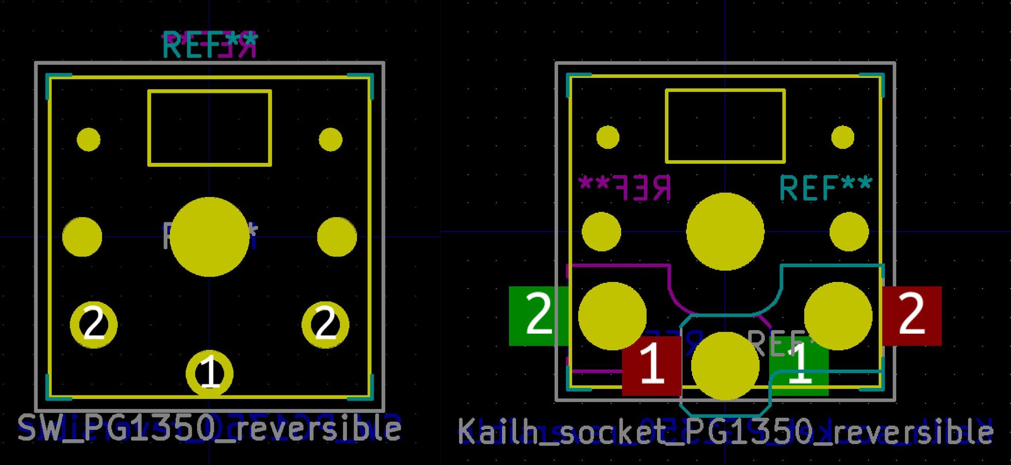
The big topic that’s likely to come up is hot swap sockets. These are small plastic sockets that solder onto a pair of SMD pads which allow us to temporarily slot a switch into a PCB. A keyboard’s worth of switches adds up quickly, and it’s nice to be able to re-use them between builds. Thankfully hot swap sockets are easy to support with reversible footprints. You just add some extra holes and pads instead of an extra through hole.
One interesting element that emerges from key switches square shape is that MX and Choc switches put all their posts and pins in the center of the switch or off to one side. Half the footprint is essentially blank. This can be a nice place to put other components. Most switches these days specifically have a small window cutout for shining LEDs up through the key and a translucent keycap. This empty space can also give you some room to place your diodes.
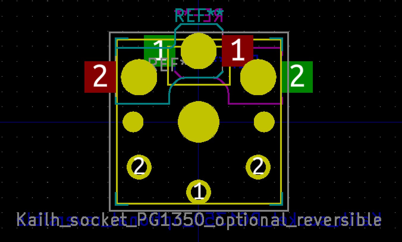
If you’re willing to skip the LEDs and put the diodes elsewhere in your build, there are some interesting options you can enable. The first is making your key switch footprints support both hot swap and soldered configurations. Face up offers the hot swap socket pads, and face down gives you the option of permanently soldering a switch into a through hole pin.
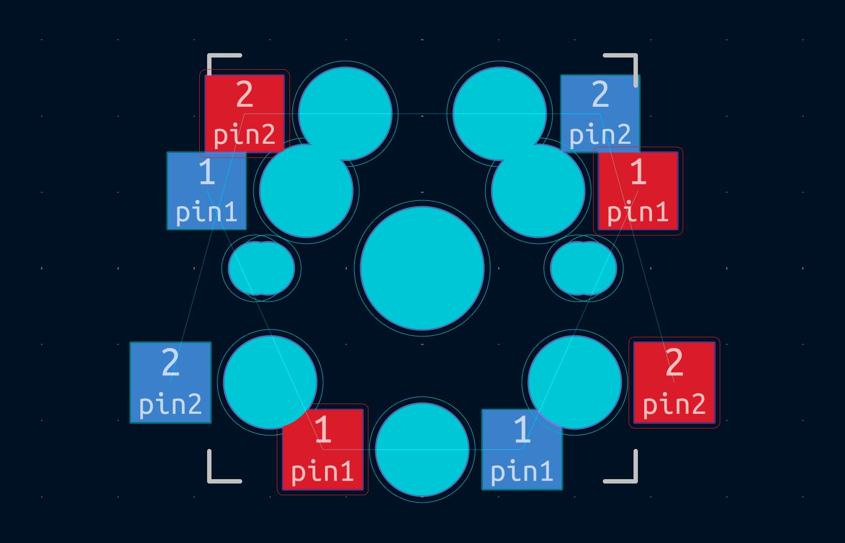
Alternatively, you can also offer up a combo MX and Choc footprint. They have enough in common that they won't get in the way of each other if you do the same face-up / face-down dance. The catch is that MX keycaps are generally 19x19mm, where Choc keycaps are around 18x17mm. This means that your Choc keyboards will have to be "MX Spaced" with the keys a bit further apart.
Leveraging the sorts of dual-purpose footprints can be great for commercial kits, but you need to keep in mind what the main focus of your keyboard build is going to be. If you're already planning on using hotswap sockets, including the through hole pins just clutters up your board layout and makes the positioning of your diodes that much tighter. The footprint flexibility usually comes at the cost of literal keyboard stability. MX keys have a larger center plastic post than Choc switches for example, those smaller switches are liable to wiggle around a bit more on your PCB. There are some absolutely clever all-purpose switch footprints floating around, but they often assume you're using a switch plate to provide added stability. Personally when I'm building a Choc v1 keyboard I just stick with the standard reversible hotswap socket footprint and enjoy the extra space to place LEDs, diodes, and anything else I'd like to work with.
Thankfully the physical MX and Choc key switches are relatively simple in their wiring. All that happens when you press a key down is that the two pins of the switch are connected together. As mentioned in the earlier diode section, you need to make sure those are pointed in the right direction, but fortunately there's not much else going on in the centerpiece of your keyboard.
For a good overview of MX and Choc footprint options, I recommend taking a look at some of the examples in daprice's keyswitches library. These KiCAD footprints haven't been converted for Ergogen, ceoloide's ergogen-footprints can usually recreate those examples if you set the flags right. Each file has a params section at the top which lets you know what it can do.
RGB LEDs
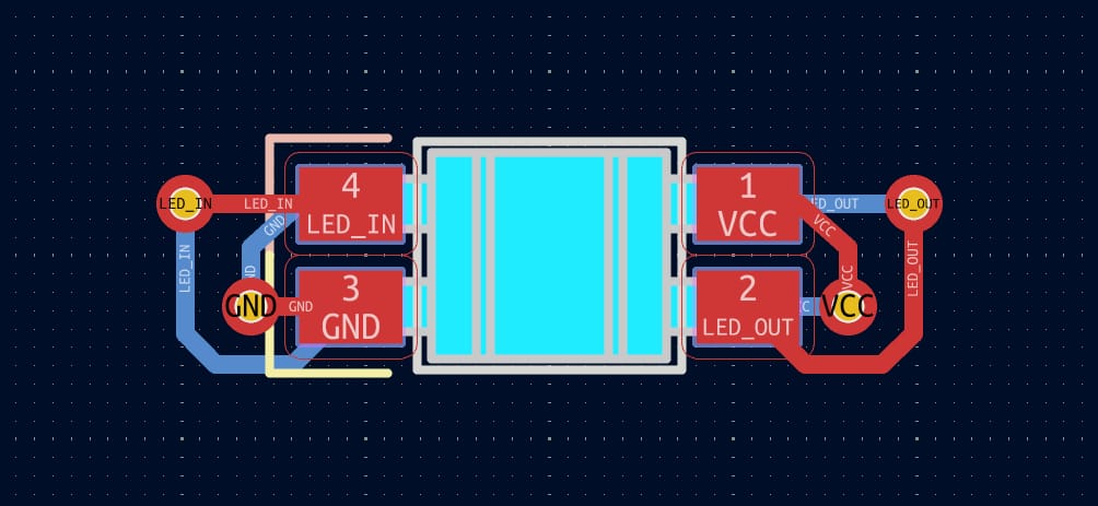
led:
  what: ceoloide/led_sk6812mini-e
  where: true
  params:
    reversible: true # Place a second footprint on the opposite side, rotated 180 degrees.
    include_traces_vias: true # Generate a few helper traces and vias to deal with mismatched pins on the flipped side.
    P1: VCC
    P2: LED_OUT
    P3: GND
    P4: LED_IN
Speaking of LEDs, these little serial SK6812 Mini-E RGB LEDs have been surprisingly fun to work with. They’re SMD components which are meant to mount on the bottom of your PCB. They shine up through a small cutout hole in the PCB, and then up though a transparent window in the key switch. The “Mini-E” variety has large SMD legs on it to make them relatively easy to hand-solder. (Make sure you get the right variant, some other SK6812s have a different pinout.)
I spoke a bit about how to use these in Ergogen as part of my RevXL writeup. Each LED receives a bit of serial data from a data-in pin telling it which color it should shine. It then has a data-out pin passing that signal onto the next LED. They get wired up roughly like a Christmas tree. The Ergogen syntax can get a bit verbose, so go read that full writeup for some pointers..
Thankfully when it comes to making these RGB LEDs reversible, there's nothing too complex going on. Much like SMD diodes, all you need to do is put a pair of pads on the front and back of your PCB and make sure the LEDs are oriented correctly on the reverse side of the PCB. Ceoloide's led_sk6812mini-e footprint enables this with the reversible: true parameter. Actually routing these reversible LEDs is another story. You need to use a decent amount of vias to make sure both sides of the keyboard get the right signals. If you set ceoloide's footprint to include_traces_vias: true, you get a few built in traces and vias to get you started.
TRRS Headphone Jacks

I plead the fifth?
I've never designed a split wired keyboard before. I'm a little hesitant to provide design guidance without at least some relevant experience. Ceoloide's footprint should get you pretty far. Make sure to check the headers for the parameters that are available.
JST Battery Socket & Power Switch
battery:
  what: ceoloide/battery_connector_jst_ph_2
  where: matrix_inner_num # Pick a point close to where you need it.
  adjust: # Use adjust to move it to where you need it to go.
    shift: [1kx+5.75+5.4,0ky-34]
    rotate: -90
  params:
    reversible: true # Enable reversibility

switch:
  what: ceoloide/power_switch_smd_side
  where: matrix_inner_num # Pick a point close to where you need it.
  adjust: # Use adjust to move it to where you need it to go.
    shift: [1kx+5.75+12.5,0ky+4.25]
    rotate: 0
  params:
    reversible: true
    from: BAT_P
    to: RAW
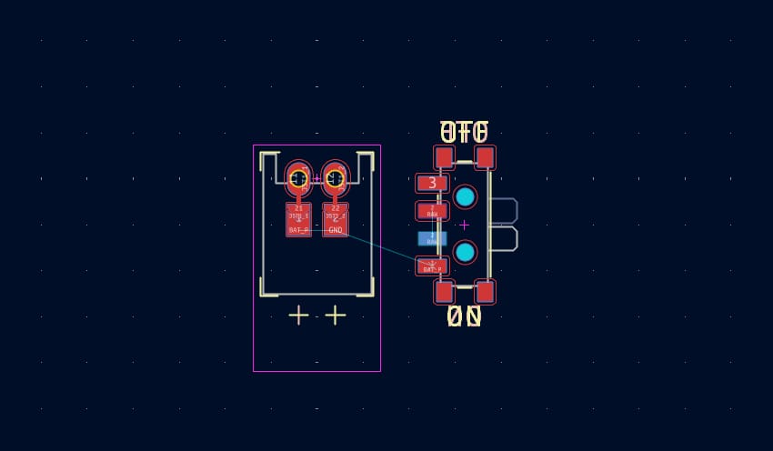
These quick connect JST battery sockets were featured pretty extensively in the introduction to this section. While the three-hole approach is valid, most builds I've seen use jumper pads. They help keep your builds nice and symmetrical across the two halves. Thankfully ceoloide’s footprints make this nice and easy. When leveraging the battery_connector_jst_ph_2 footprint, just set reversible: true and you’re off to the races.
A race that leads you directly to the power switch. Ceoloide's power_switch_smd_side footprint also has a reversible: true param. It simply places a second copy of the SMD switch footprint on the back of the PCB. Make sure you use vias or something similar to wire up both sides of the switch.
As discussed in the wireless section of this guide, batteries need to make a complete loop to the RAW and GND pins in order to power the microcontroller. If either the BAT_P or BAT_N leads become disconnected, the battery will stop working. You can set the switch params as from: BAT_P and to: RAW or from: BAT_N and to: GND. In this particular example, cutting the BAT_P lead was a bit easier for all the routing.
OLED and Nice!View Displays
oled:
  what: ceoloide/display_ssd1306
  where: matrix_inner_num
    adjust:
      shift: [1kx+5.75,0ky-9]
    params:
      reversible: true # Enable reversibility
      # SDA, SCL, VCC, and GND pin I2C definitions set by default.

niceview:
  what: ceoloide/display_nice_view
  where: matrix_inner_num
    adjust:
      shift: [1kx+5.75,0ky-9]
    params:
      reversible: true # Enable reversibility
      # MOSI, SCK, VCC, GND, and CS pin SPI definitions set by default.
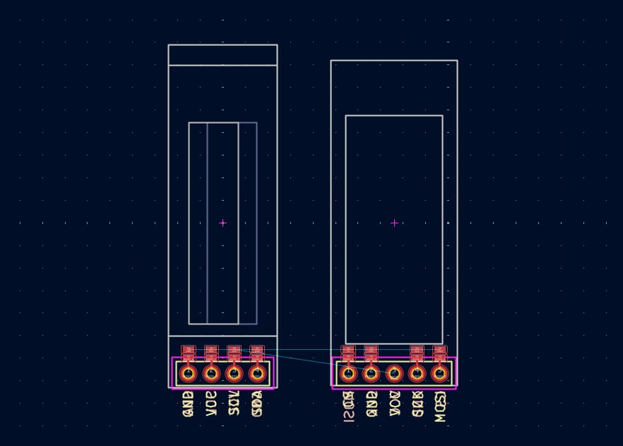
The DIY community has largely coalesced around two main displays for keyboard builds. Wired QMK builds often feature a generic SSD1306 0.91" OLED display, while wireless ZMK builds typically use the Nice!View “transflective LCD”. The Nice!View is a bit more expensive, but OLED displays are a significant power drain on wireless builds.
Both of these displays mount nicely over a Pro Micro’s footprint. The OLED display uses a four pin footprint and I2C to communicate to the microcontroller, while the Nice!View uses a five pin footprint and SPI. Some microcontrollers use hardware based serial communication requiring the use of specific pins, so your ability to remap these displays pins will vary. Since most footprints are already using jumper pads to re-route the power lines, there's usually jumpers to move the data lines as well.
Ceoloide’s also got these covered. display_ssd1306 for the OLED displays, and display_nice_view for the Nice!View. Both of them support reversible: true to add the jumper pads. (Since the Nice!View has an odd number of pins, the middle VCC pin doesn't need a jumper.)
Rotary Encoders
rotary:
  what: ceoloide/rotary_encoder_ec11_ec12
  where: matrix_inner_num
  adjust:
    shift: [1kx+5.75,0ky-47]
  params:
    reversible: true # Technically reversible already, just doubles the silkscreen.
   S1: rotdiode # Intersecting colrow net connecting to the diode below. (Could be swapped with S2 if needed.)
   S2: col6 # Integrate rotary encoder pushbutton into matrix at Col6-Row1. (Could be swapped with S1 if needed.)
   A: rotA
   B: rotB
   C: GND

# One-off diode for rotary encoder pushbutton. Required for a QMK build.
# On a ZMK build, you can also wire the pushbutton up to a GPIO and GND.
# Solder diode on opposite side as the encoder.
rotary_diode:
  what: ceoloide/diode_tht_sod123
  where: matrix_inner_num
  adjust:
    shift: [1kx+5.75,0ky-47]
  params:
    reversible: true # Includes SMD pads on both sides of the PCB.
    from: rotdiode # Intersecting column-row net connecting to the switch. (Don't swap with 'to'.)
    to: row1 # Integrates rotary encoder pushbutton into matrix at Col6-Row1 (Don't swap with 'from')
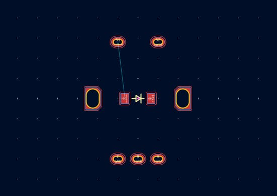
We're getting towards the end of the common keyboard hardware. Before wrapping things up with microcontrollers, I briefly wanted to discuss rotary encoders. These are those little knobs that you see on some keyboards. If you twist them clockwise they trigger one command, and if you twist them counter-clockwise they trigger a different command. The EC11 encoder variant also has a pushbutton action to trigger a third command. The shorter EC12 model lacks this push button and just has the rotations.
Their footprints are interesting because they're completely symmetrical. There's two mounting pins, three pins for the rotation action, and then the EC11 has a final additional pair of pins for the pushbutton action.
The pushbutton portion is straightforward enough. It works like a standard reset pushbutton or keyboard switch. When you push in on the EC11, from: and to: get connected together. (Or S1: and S2: on ceoloide's footprint.) Depending on your keyboard firmware, you can wire the pushbutton pins up as part of your keyboard matrix, or connect it to any free GPIO and GND. (ZMK supports having a mixture of keyboard matrix and directly-driven pins. With QMK, you'll need to integrate the encoder into your matrix if you're using one.) Just like our reset switch, the important thing here is that the pins are being bridged. The order of the pins doesn't matter.
For the rotating portion, the EC11 and EC12 use three pins often labeled A, B, and C. A and B are connected to two GPIO pins, and C is connected to GND. The knob basically works like a pair of push buttons. When you rotate it, the rotary encoder will briefly connect A and GND, then connect B and GND. By watching the pattern of the signals, your microcontroller can determine whether the knob’s rotating clockwise or counter-clockwise.
Through either fortune or foresight, the physical layout of the pins is A-C-B. The GND pin rests right in the vertical center of the footprint. When you mount the encoder on the back side, things get flipped so it’s now wired up B-C-A.
If you just left things alone here, both encoders would still work. The secondary side's encoder would just have its clockwise and counter-clockwise commands flipped. Thankfully both QMK and ZMK allow us to remap the A and B GPIO pins differently for the primary and secondary halves of the keyboard, so you don't have to keep track of the flip-flopped commands.
Ergogen’s default EC11 footprint doesn’t have a reversible: option for rotary.js since the rotary encoder footprint is already inherently reversible. Ceoloide’s rotary_encoder_ec11_ec12 footprint does have a reversible: true option, but all it does is draw the silkscreen on both sides. It does have a handy include_momentary_switch_pads: flag to hide the EC11’s extra pins if you’re planning on using the EC12 however. (Update: It looks like the B and C pins might be switched on ceoloide's footprint as of right now. Double-check that the C ground pin is in the center.)
Pro Micro, Nice!Nano, and Other Compatible Microcontrollers
nicenano:
  what: ceoloide/mcu_nice_nano
  where: matrix_inner_num # All of the microcontroller parts are anchored to the top-right key as a starting place.
  adjust:
    shift: [1kx+5.75,0ky-6] # A large shift is applied to move these parts into place.
  params:
    reversible: true # Enable reversibility
    reverse_mount: true # Microcontroller face down.
    P21: col1
    P20: col2
    P19: col3
    P18: col4
    P15: col5
    P14: col6
    P16: rotA
    P10: rotB
    P1: CS
    # P0: MISO Nice!View only uses an output pin, not an input pin.
    P2: MOSI
    P3: SCK
    P4: row5
    P5: row4
    P6: row3
    P7: row2
    P8: row1
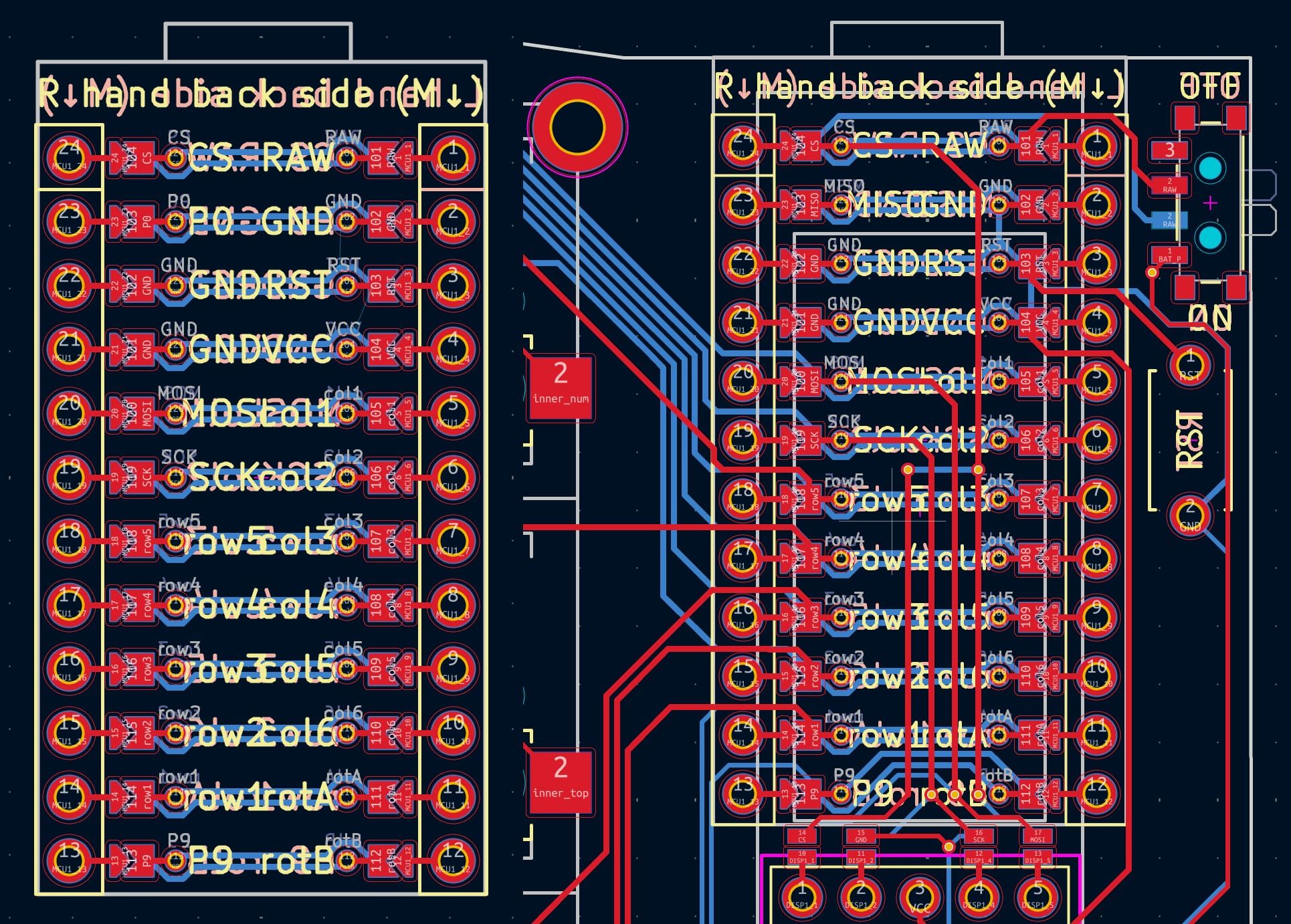
Alright, the moment you’ve been waiting for. Microcontroller footprints are the most complicated aspect of reversible PCBs. They build on all the concepts I described above, so I saved the best for last.
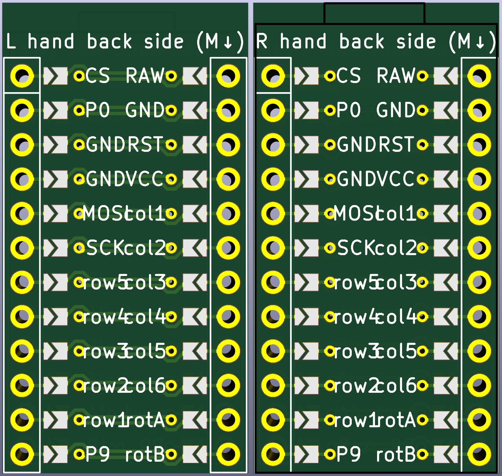
Before we get started however, it’s worth noting there’s no “Right” way to make a reversible PCB. There are plenty of different ways to make a microcontroller reversible. Some of it comes down to taste, and some of it comes down to how much you want to solve in hardware or tweak in software.
The big issue with microcontroller footprints is that the power and ground pins aren't remappable in software. You're always going to be piping 5v or 3.3v out of one side of the microcontroller. (This isn't a Pro Micro limitation either, every microcontroller typically has an asymmetrical pinout.) We need a way to make those power pins route properly whether our keyboard PCB is in the standard or reverse orientation.
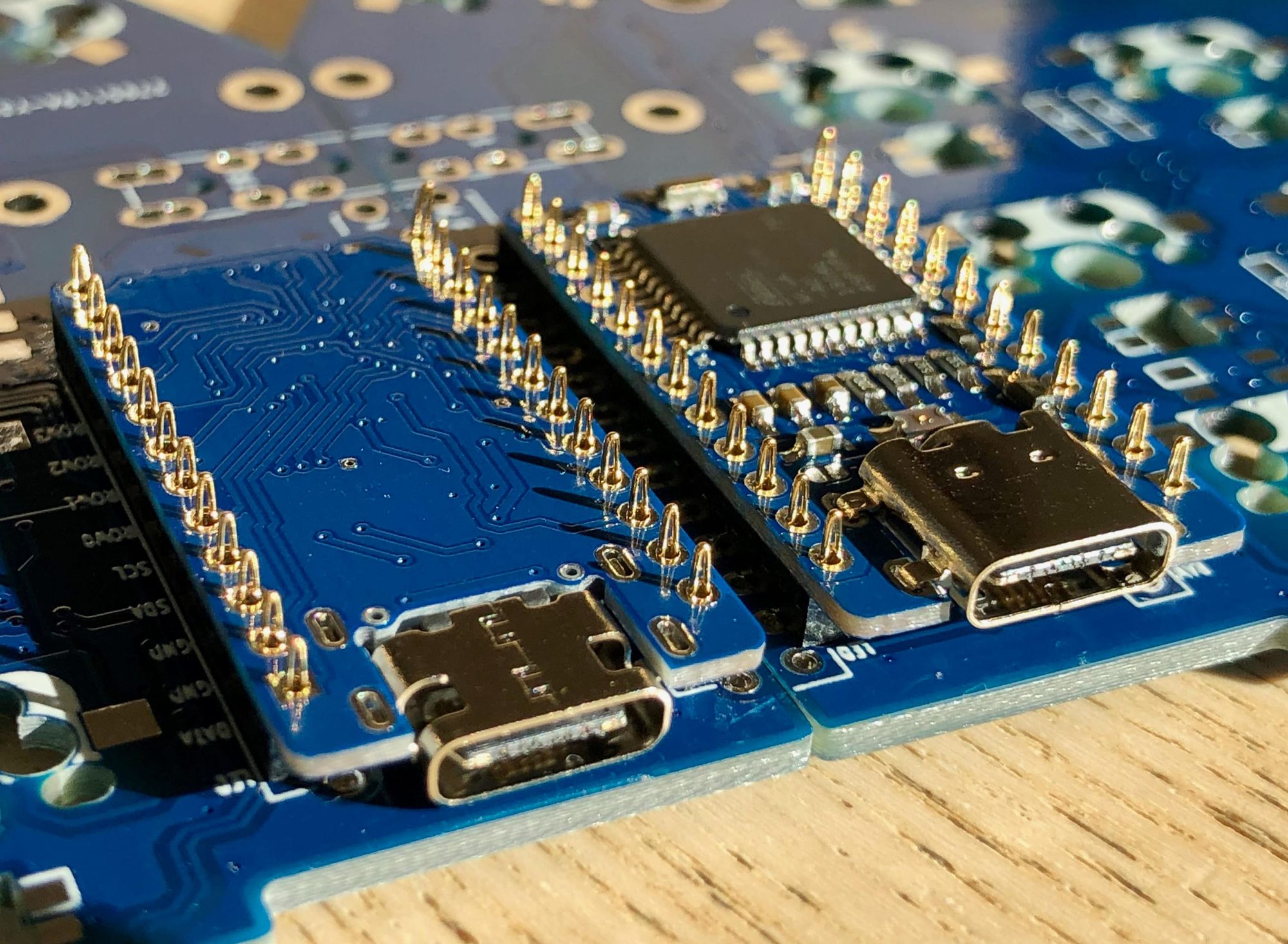
The quickest way to solve this problem is to flip the Pro Micro itself. If you mount the Pro Micro face-up on one side of your split keyboard and face-down on the other side, the pinout will stay the same. This isn't common for a variety of mostly aesthetic and physical reasons. People don't like the asymmetry of the build, and the Pro Micro's chips and USB port will be in slightly different places on the reverse side of the keyboard. This makes things like positioning displays or batteries more tricky, and case design becomes a bit more complex. It's always an option, but a relatively rare one. The majority of keyboard builders like to orient the microcontrollers face-down on both halves. (Although you should always double-check their docs.)
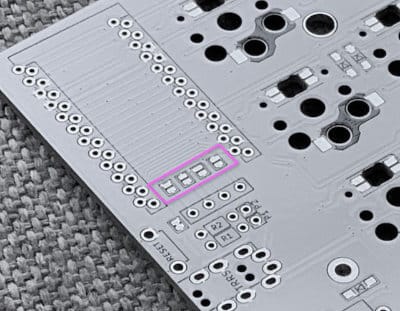
The first split keyboard I built was the wired Sofle. To make its PCB reversible, Josef Adamčík took a dual-through hole approach. To get around the issues caused by a flipping PCB, he literally includes two overlapping Pro Micro footprints. One is meant to be used for the left side of the keyboard, and the other's meant to be used for the right side of the keyboard. This allows both of the microcontrollers to be mounted face down. The keyboard is relatively symmetrical, with one of the microcontrollers only nudged over by a few millimeters.
This dual-through hole approach was common a few years ago, but the jumper pad approach has become a bit more widely adopted these days. It's what ceoloide's community library uses, so it's what we're going to focus on today. (Ergogen's default Pro Micro footprint does not have a reversible option.)
It's worth noting that while the Nice!Nano is explicitly meant to be pin compatible with the Arduino Pro Micro, ceoloide still offers up footprints specifically for the Pro Micro, the Nice!Nano, and the nRF52840 Supermini. The Nice!Nano and the Supermini have additional interior pins not found on the classic Pro Micro, and ceoloide has some optional (default disabled) parameters to show those pins. Use whichever footprint matches what microcontroller you plan to use, but the overall strategy here won't change between microcontrollers.
Turning on reverse_mount: true makes our microcontroller orient face-down. reversible: true adds a jumper pad for every pin on the board. If you solder one set of jumper pads, the footprint will have it's stock (face-down) pinout. If you solder the other set of pads, it will flip the pinout.
Make sure to clearly label which set of jumper pads need to be soldered shut for each side of your keyboard.
Other people might build your keyboard. You might build another copy of your keyboard a year from now. Don't assume you'll remember or have the patience to double-check your PCB. Make sure you make it clear if your microcontroller should be mounted face-up or face-down, and which jumper pads you need to solder for each side of the keyboard. Sorry, I don't think I made that clear enough.
MAKE SURE YOU PUT A SILKSCREEN ON YOUR KEYBOARD INDICATING HOW THE MICROCONTROLLER IS MOUNTED AND WHICH JUMPER PADS TO SOLDER.
Techniques for how to label your keyboard vary. Some people will spell out, "This is the left half of the keyboard. Mount the microcontroller face down and solder such-and-such pads."
Ceoloide's footprint includes a small note at the top, and includes labels for the microcontroller's pinout. The pins are also usually silkscreened on the microcontroller itself, so you can double check you've got the right orientation as you get everything situated. His Pro Micro footprints have you solder the jumper pads on the opposite side as the microcontroller. It makes everything a bit easier to get to with your soldering iron.
Anyways, now that those warnings are out of the way, time to discuss how we're going to wire this bad boy up. Each pin on the microcontroller is set up like:
Through Hole <-> Front Jumper <-> Via <-> Back Jumper <-> Through Hole
If you solder the front jumper shut, that signal goes to the left through hole. If you solder the back jumper shut, that signal goes to the right through hole.
All the nets for the microcontroller through hole pins are set up such that they only connect to the exterior half of the jumper pads beside them. The actual keyboard nets for things like your switch matrix, displays, and rotary encoders will be on the interior jumper pads.
Because the front jumper and the back jumper are connected through a via, you should have a convenient signal on the front or back of your keyboard to route to. Things will just be a bit more cramped than if you could route to the through holes themselves.
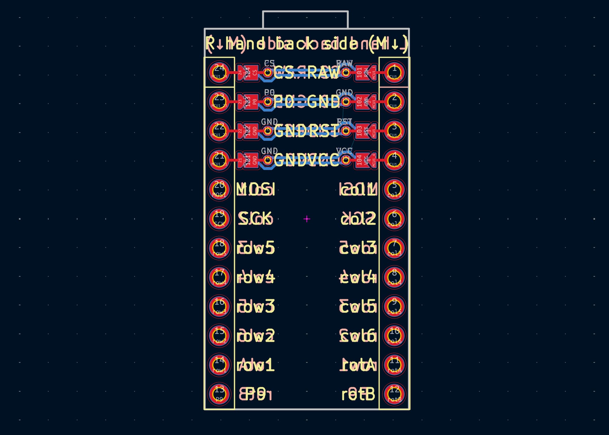
One thing that can help clear up some routing space is the only_required_jumpers: parameter. If you set this feature to true, the footprint will only have jumpers for the first four rows. (RAW and P1, GND and P0, GND and RST, GND and VCC.) These jumpers are mandatory since the power pins can't be remapped in software. It'll be on you to tell QMK or ZMK that "Column 3 is connected to P2 on the primary half, and P21 on the secondary half." One's more work for you on the routing side, the other's more work for you on the software side. For what it's worth, once you're soldering, there's not a huge difference between soldering 8 pads or 24 pads.
That's... pretty much it. The cluster of jumper pads and traces looks a little daunting when you first look at it, but it starts to make a bit more sense once you know the theory behind it. Just triple-check everything and put a note on your silkscreen about the relevant details.
XIAO, RP2040-Zero, and Other Microcontrollers
The XIAO nRF52840 and the RP2040-Zero microcontrollers have similarly asymmetrical pinouts. You'll need to use jumper pads to re-route some of the power pins around. The XIAO nRF52840 also has offset pins for the battery, so you'll need a second mirrored cutout on the opposite side for when you're reverse mounting it. It's nothing out of the realm of possibility, but I haven't seen any Ergogen-ready reversible footprints for non-Pro Micro microcontrollers. If you're looking to incorporate one into your build, maybe ask around the Ergogen Discord and see if anyone's got a footprint they can lend you.
Example Config
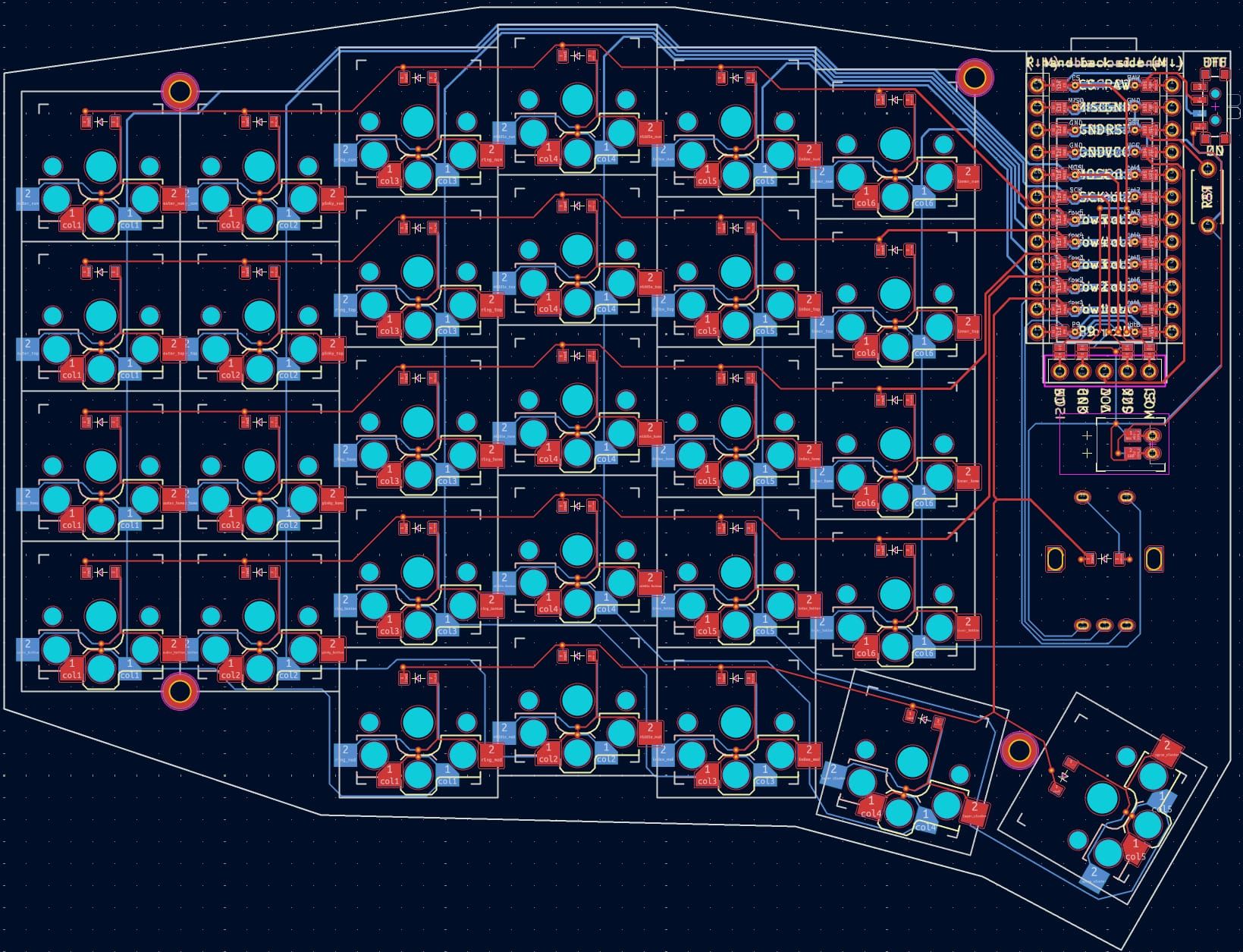
Now that we know how each of the individual footprints work, let's see how everything comes together!
meta:
  engine: 4.1.0
units:
  # Web View Resizing
  $default_width: cx
  $default_height: cy
  # Proxy Spacing Variables
  kx: cx
  ky: cy
  # Padding Variables
  px: kx + 4
  py: ky + 4
points:
  zones:
    # The primary 6x4 key matrix, plus 3 modifiers.
    matrix:
      # Position in center of KiCAD workspace.
      anchor:
        shift: [100, -100]
      # Choc spacing
      key:
        padding: 1ky
        spread: 1kx
      columns:
        # Hide the first two mods and the last mod.
        # Provide a Sofle-like column stagger.
        outer:
          rows.mod.skip: true
          key.column_net: col1
        pinky:
          rows.mod.skip: true
          key.column_net: col2
        ring:
          key:
            stagger: 5
            column_net: col3
          rows.mod.column_net: col1
        middle:
          key:
            stagger: 2.5
            column_net: col4
          rows.mod.column_net: col2
        index:
          key:
            stagger: -2.5
            column_net: col5
          rows.mod.column_net: col3
        inner:
          rows.mod.skip: true
          key:
            stagger: -2.5
            column_net: col6
      rows:
        # Four main rows, one partial row.
        mod:
          row_net: row1
        bottom:
          row_net: row2
        home:
          row_net: row3
        top:
          row_net: row4
        num:
          row_net: row5
    # Thumb cluster for Layer and Space keys.
    thumbs:
      # Choc spacing
      key:
        padding: 1ky
        spread: 1kx
      # Place thumbs where the inner mod would go.
      anchor:
        ref: matrix_inner_mod
        shift: [2, -2]
      columns:
        # Fan thumbs out by -15 degrees.
        layer:
          key:
            splay: -15
            column_net: col4
        # Spacebar uses a 1.5 wide key.
        space:
          key:
            width: 1.5kx
            splay: 75
            shift: [2.5,-3.25]
            column_net: col5
      rows:
        # Thumbs only have one row.
        cluster:
          row_net: row1
outlines:
  keys:
    - what: rectangle
      where: true
      size: [kx-0.5,ky-0.5]
  board:
    - what: polygon
      operation: stack
      points:
        - ref: matrix_outer_num
          shift: [-0.5px,0.5py]
        - ref: matrix_ring_num
          shift: [-0.5px,0.5py]
        - ref: matrix_middle_num
          shift: [-0.5px,0.5py]
        - ref: matrix_middle_num
          shift: [0.5px,0.5py]
        - ref: matrix_inner_num
          shift: [0.5px,0.5py]
        - ref: matrix_inner_num
          shift: [0.5px+27,0.5py] # Eyeballed +27 to give room for the microcontroller.
        - ref: thumbs_space_cluster
          shift: [0.5px,-0.5py]
        - ref: thumbs_space_cluster
          shift: [-0.625px,-0.5py] # This technically probably should have been 0.75 for a 1.5u switch, but it looked a little weird.
        - ref: thumbs_layer_cluster
          shift: [0.5px,-0.5py]
        - ref: thumbs_layer_cluster
          shift: [-0.5px,-0.5py]
        - ref: matrix_ring_mod
          shift: [-0.5px,-0.5py]
        - ref: matrix_outer_bottom
          shift: [-0.5px,-0.5py]
  preview:
    - name: board
    - operation: subtract
      name: keys
pcbs:
  tutorial:
    outlines:
      main:
        outline:
          board
    template: kicad8 # Include KiCAD 8 template to use ceoloide footprints.
    footprints:
      # Hotswap Choc v1 switches.
      choc:
        what: ceoloide/switch_choc_v1_v2
        where: true
        adjust: # Choc v1 switches are symmetrical and can be mounted rotated 0 or 180 degrees.
          rotate: 180 # Rotating them 180 degrees will shine the LED window through the top half, matching most shine-through keycaps.
        params:
          reversible: true # Enable reversibility
          hotswap: true # Hotswap sockets instead of through holes
          include_keycap: true # Show keycap outline on non-fabbed Dwgs.User layer.
          keycap_width: kx # Keycap Width
          keycap_height: ky # Keycap Height
          include_corner_marks: true # Dwgs.User markings for edge of Choc switch.
          choc_v1_support: true # Enable v1 support.
          choc_v2_support: false # Disable v2 support so v1 switches will be a bit tighter in the PCB.
          from: "{{column_net}}" # Column net to Microcontroller. (Can be swapped with 'to' if needed.)
          to: "{{colrow}}" # Intersecting column-row net connecting to diode. (Can be swapped with 'from' if needed.)
      # SMD Diodes
      diode:
        what: ceoloide/diode_tht_sod123
        where: true
        adjust:
          shift: [0, 5]
        params:
          reversible: true # Includes SMD pads on both sides of the PCB.
          from: "{{colrow}}" # Intersecting column-row net connecting to the switch. (Don't swap with 'to'.)
          to: "{{row_net}}" #  Row net connecting to Microcontroller. (Don't swap with 'from'.)
      # Nice!Nano Compatible Microcontroller
      nicenano:
        what: ceoloide/mcu_nice_nano
        where: matrix_inner_num # All of the microcontroller parts are anchored to the top-right key as a starting place.
        adjust:
          shift: [1kx+5.75,0ky-6] # A large shift is applied to move these parts into place.
        params:
          reversible: true # enable reversibility
          reverse_mount: true # Microcontroller face down.
          P21: col1
          P20: col2
          P19: col3
          P18: col4
          P15: col5
          P14: col6
          P16: rotA
          P10: rotB
          P1: CS
          # P0: MISO Nice!View only uses an output pin, not an input pin.
          P2: MOSI
          P3: SCK
          P4: row5
          P5: row4
          P6: row3
          P7: row2
          P8: row1
      # Nice!View transflective LCD.
      niceview:
        what: ceoloide/display_nice_view
        where: matrix_inner_num
        adjust:
          shift: [1kx+5.75,0ky-9]
        params:
          reversible: true # Enable reversibility
      # JST battery header.
      battery:
        what: ceoloide/battery_connector_jst_ph_2
        where: matrix_inner_num
        adjust:
          shift: [1kx+5.75+5.4,0ky-34]
          rotate: -90
        params:
          reversible: true # Enable reversibility
      # A power switch.
      power:
        what: ceoloide/power_switch_smd_side
        where: matrix_inner_num
        adjust:
          shift: [1kx+5.75+12.5,0ky+4.25]
          rotate: 0
        params:
          reversible: true
          from: BAT_P
          to: RAW
      # Two pin through hole pushbutton for resetting your microcontroller.
      # Double tap to flash new firmware.
      reset:
        what: ceoloide/reset_switch_tht_top
        where: matrix_inner_num
        adjust:
          shift: [1kx+5.75+11.65,0ky-6]
          rotate: 90
        params:
          reversible: true # Reversible only doubles the silkscreen.
          # Default params include from: GND to: RST
      # EC11 Rotary Encoder
      rotary:
        what: ceoloide/rotary_encoder_ec11_ec12
        where: matrix_inner_num
        adjust:
          shift: [1kx+5.75,0ky-47]
        params:
          reversible: true # Technically reversible already, just doubles the silkscreen.
          S1: rotdiode # Intersecting colrow net connecting to the diode below. (Could be swapped with S2 if needed.)
          S2: col6 # Integrate rotary encoder pushbutton into matrix at Col6-Row1. (Could be swapped with S1 if needed.)
          A: rotA
          B: rotB
          C: GND
      # One-off diode for rotary encoder pushbutton. Required for a QMK build.
      # On a ZMK build, you can also wire the pushbutton up to a GPIO and GND.
      # Solder diode on opposite side as the encoder.
      rotary_diode:
        what: ceoloide/diode_tht_sod123
        where: matrix_inner_num
        adjust:
          shift: [1kx+5.75,0ky-47]
        params:
          reversible: true # Includes SMD pads on both sides of the PCB.
          from: rotdiode # Intersecting column-row net connecting to the switch. (Don't swap with 'to'.)
          to: row1 # Integrates rotary encoder pushbutton into matrix at Col6-Row1 (Don't swap with 'from')
      # A few stray mounting holes.
      # There's probably some more-optimal placement.
      # But here's some examples to get you started.
      # These default M2 screw holes are small enough to fit between Choc v1 switches.
      mount_top_left:
        what: ceoloide/mounting_hole_plated
        where: matrix_outer_num
        adjust.shift: [0.5kx, 0.5ky]
      mount_bottom_left:
        what: ceoloide/mounting_hole_plated
        where: matrix_outer_bottom
        adjust.shift: [0.5kx, -0.5ky]
      mount_top_right:
        what: ceoloide/mounting_hole_plated
        where: matrix_inner_num
        adjust.shift: [0.5kx, 0.5ky-1]
      mount_bottom_right:
        what: ceoloide/mounting_hole_plated
        where: thumbs_space_cluster
        adjust.shift: [0kx, 0.5ky+2.25]
If you’d like to take a closer look at the routing, you can download the config and finished PCB from GitHub. As a disclaimer, I do want to note I've never fabricated or built the above keyboard. The general principles should be sound, but I can't guarantee some of the parts won't bump up against each other if you try building this particular PCB config. This tutorial keyboard was loosely styled on the Sofle Choc, and there's much better kits available for it online at most ergonomic keyboard vendors.
Conclusion
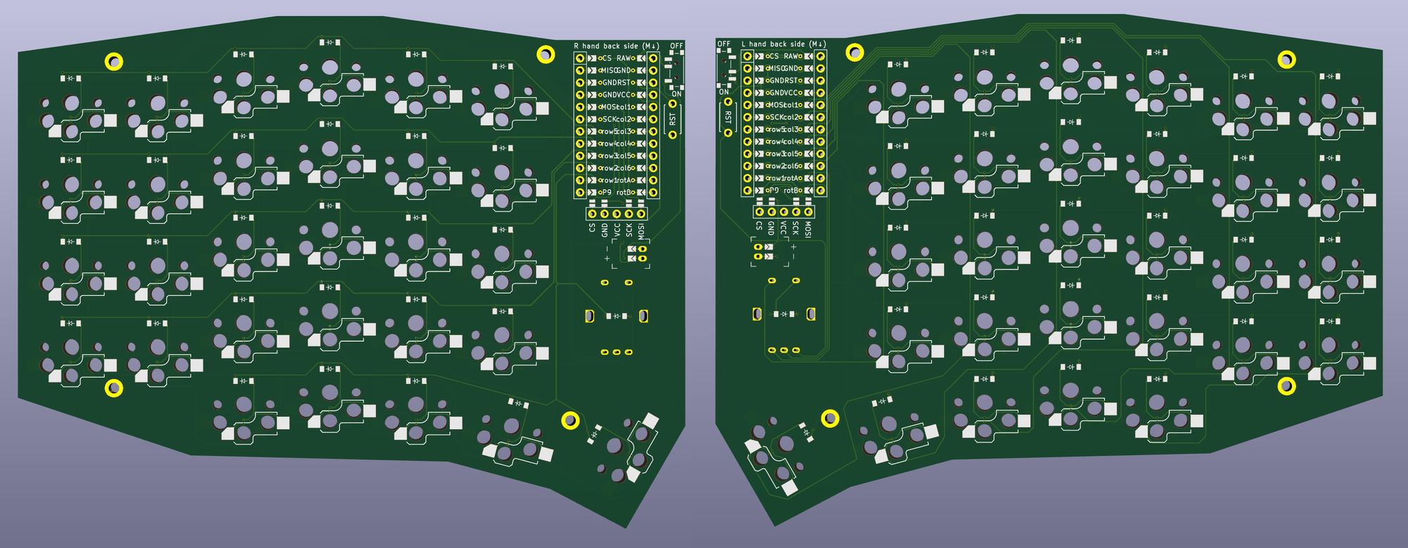
Hopefully that gives you an idea of where to get started with a split keyboard design. As much as I love a good unibody, I'm glad I was finally able to package some of this information together.
If you jumped straight into this chapter, make sure to give Let's Design a Keyboard with Ergogen v4 a look. It goes into more step-by-step detail about how to position keys in Ergogen, route a keyboard in KiCAD, and get your finished design fabricated.
Thanks to ceoloide, Saixos, and the rest of the Ergogen Discord for providing feedback, guidance, and oh so much spell checking for this writeup. As always, give me a shout if you managed to build a split keyboard with the help from this guide. I'm usually hanging around the Ergogen Discord, and you can also find me on Mastodon. If you're feeling extra generous, I've got a Cash App tip jar.