Congratulations, you've made it to Part 3! If you've been following along with this series so far, you should have an Ergogen config file with defined units, a keyboard layout specified by points, and a board shape created from an outline. If you're just joining us and this all sounds like gibberish, feel free to hop back to the introduction.
Before we dive straight into discussing how to design a PCB, we need to have a brief side discussion about microcontrollers and keyboard matrixes. I promise I'll try to keep this short.
What's a Microcontroller?
It's a controller but... micro?
Okay, in all seriousness, a microcontroller is a small reprogrammable chip designed to work in embedded applications. It differentiates itself from more powerful computing devices by generally lacking a traditional operating system. Microcontrollers get flashed with a single program, and will run that script every time it powers up until you flash it with a new program. Microcontrollers also generally have hardware designed to interact with low level hardware components. Instead of focusing on powering a single screen and running a variety of apps, microcontrollers can power LEDs, read sensor states, and drive small motors.
The most popular and hobbyist friendly microcontroller platform has been the Arduino family of boards. Custom mechanical keyboards have been leveraging the Arduino Pro Micro for years now, although different variant boards also exist. Microcontrollers like the Elite-C have Arduino compatibility while offering slightly different hardware capabilities. More recently, Seedsudio's XIAO line of boards and the Raspberry Pi foundation's RP2040 boards have also made inroads into the mechanical keyboard scene.
No matter which board you're working with, they all tend to behave in the same way. If you ever played with electric circuit kits as a kit, you should have a rough idea what's going on here. Microcontrollers have a variety of "pins" on them, all with their own specific purpose and usage type.
The most basic pins are "Ground" and "VCC". These pins are essentially the positive and negative end of a AA battery. If you connect the positive pin of an LED to VCC, and the negative end to Ground (GND), then congratulations. You've got light.
The majority of pins on an Arduino are known as "General Purpose Input/Output" pins. These are pins that can be controlled via software for you guessed it, general input or output tasks. If you connected the positive end of your LED to GPIO 1 and the negative end to your GND, your LED wouldn't light until you sent a software command which says, "Turn on GPIO 1".
Conversely, we can also use this same basic setup for wiring inputs. If instead of an LED we put a basic switch in between GPIO 2 and GND, it's possible to tell your software, "Perform this action when you detect someone closing the circuit between GPIO 2 and GND."
This sort of functionality is perfect for keyboards. We just need to wire up all of our switches between a GPIO pin and ground, and then write a keyboard firmware that says, "When switch 38 is flipped, type the 'A' key." Only, uh oh, the Arduino Pro Micro only has 18 GPIO pins. What do we do now?
Microcontrollers like the Arduino do have a few other tricks up their sleeves. They have analog pins which can send or receive signals that aren't a binary "on" or "off". This is useful for things like detecting light levels, but isn't exactly useful for a keyboard. We can also get into more technical ways of sending a signal. The Arduino supports I2C ("Eye-Squared-C") and SPI serial protocols for more advanced communication between devices, but this is generally only reserved for more advanced accessories like a keyboard's OLED screen.
To power a large keyboard with a handful of GPIO pins, we don't need to get a more advanced microcontroller. We need to leverage more basic electronics principles.
Enter the Matrix

Working with microcontrollers is an interesting change of pace for a lot of traditional programmers. Instead of being able to work in a purely digital world, you suddenly have to start accounting for a bunch of squishy real world physics limitations. Sometimes we can use this to our advantage though.
You probably have some passing familiarity with some basic electronics components. You've got LEDs to provide light, wires to hook things up, and resistors to... make electricity somehow less uh, electric. They resist things, right?
Diodes are one of those components everyone's heard of, but may be less clear on the details. They're a small piece of electronics that allow circuit designers to ensure that electricity is only flowing in one direction. The full details of why this is desirable is better left to full electronics engineering texts, but in short, it allows us to design circuits with very predictable and measurable flows of signals.
In all the GPIO examples I mentioned earlier, the circuits were wired with the GPIO pin generally going where the "positive" end of a battery would be, and the Ground pin was where the "negative" end of a battery would be. This isn't strictly required. We can wire a switch going from GPIO 1 to GPIO 2 and still detect in software when the button is pressed. When you introduce diodes into the picture, we can start getting very creative about wiring up multiple keys to the same GPIO pins.
Enter the keyboard matrix. This is an ancient design that essentially turns our keyboard into an intersecting grid of columns and rows. Turns out that terminology wasn't just useful for arrangement purposes. We get to leverage it here as well. If you design a keyboard matrix correctly, you can have several GPIO pins acting as the "columns", and several other GPIO pins acting as the "rows". With diodes acting as the electricity's traffic cop, we can design a circuit in which the only way GPIO 4 and GPIO 10 would both be receiving a signal is if key "A" was being held down.
The PCB section in our Ergogen config file isn't just dedicated to where the microcontroller goes on our keyboard. It also defines how the keyboard itself is wired.
Designing a Matrix
Before we actually jump into the Ergogen config, let's quickly sketch out the matrix we want to build so everyone's on the same page.
If we were building an Ortholinear keyboard, this guide would be ludicrously simple. Your up down keys are the columns, your left right keys are your rows. If our keyboard reports that Col1-Row2 is being pressed, we know it's the Z key. The unibody Sofle in this design isn't as aligned, but we can make it work.
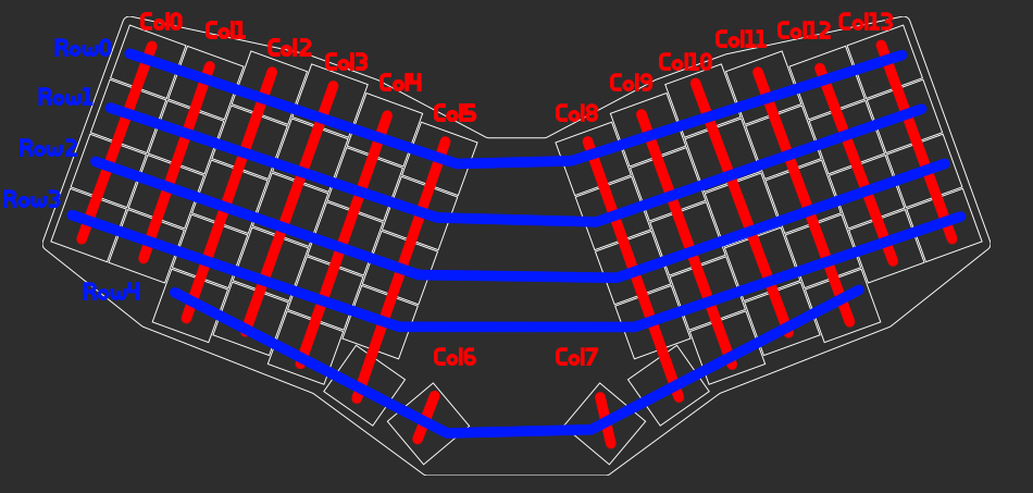
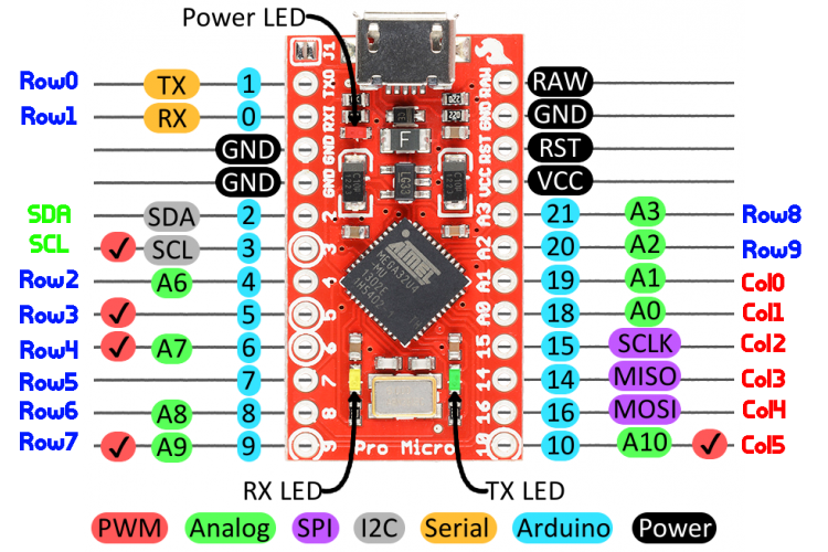
Tada, a 14 column, 5 row matrix for our Sofle. The thumbs having their own dedicated columns is a little silly, but as we saw in the Ortholinear example's spacebar, you don't have to have every matrix be the exact same size. Now that we've got the basic matrix defined, let's go back to our Arduino Pro Micro diagram and look at what the pinout for this keyboard may look like.
Welp. We've done goofed. We've got 19 rows and columns and only 18 pins. Pack it up everyone, it's been a great tutorial.
...or we could just be a little smarter about how we handle those thumbs.
By treating the thumbs as part of the inner-most columns, we can save two column pins. The mod row is essentially just shifted over by one. When the time comes to define our PCB config, we can use this layout to demonstrate how to do one-off key wiring overrides.
If we were designing a very basic keyboard, we'd be good to go at this point. However, the original Sofle Choc had support for an OLED screen. What if we wanted to add a screen to our design? The most popular OLED screen module for mechanical keyboards requires the use of the two I2C pins. Which means we're once again one pin short. Is there some way we could potentially squeeze one more pin out of our matrix?
Keyboard matrixes use an amount of pins equal to the number of columns plus the number of rows. This means that the more square your keyboard design is, the fewer number of pins you need. For example, 10 columns and 2 rows can support 20 keys across 12 pins, but 5 columns and 4 rows can support 20 keys across 9 pins.
But our layout is pretty fixed, right? We can't just magically somehow make it more square. We could free up some pins by doing something drastic like ditching the number row, but what if we could somehow just... fake a more square design? Right now we've got a 12x5 keyboard. Is there any shape that would get us closer to a square?
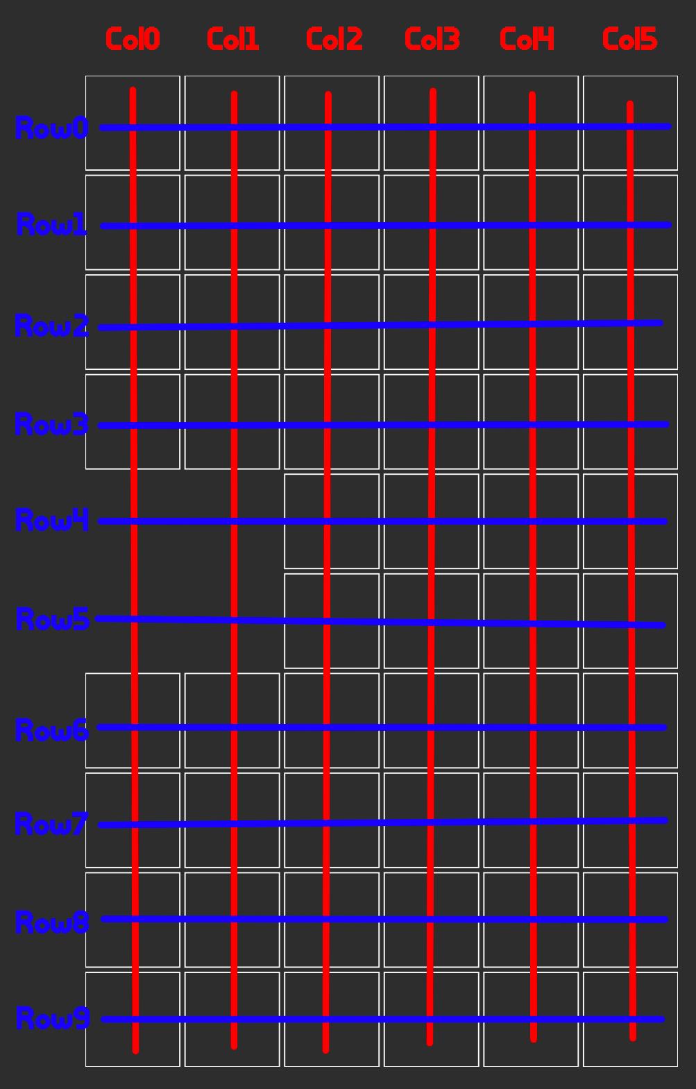
Huh. Okay. This is interesting. If you can't tell what's going on here, I took the two pieces of our keyboard and stacked them on top of each other. Gone is the nice rotate: -20 degree angle. This is an absurd keyboard bent completely in on itself. But this configuration does give us one benefit: It has 6 columns and 10 rows. 6+10=16, and would you look at that, we've managed to shave a pin off our 12+5=17 layout.
Of course, we need to figure out how to fit this into our existing wiring.

SDA and SCL I2C pins over on Pin 2 and Pin 3.Tada! Our finished keyboard matrix! This is what's known, slightly confusingly, as a "Duplex" matrix. Essentially we "bend" the columns back on each other and double the number of rows. (This doubling is where the "duplex" term comes from.) It can often help create a slightly better board geometry and save you a pin or two.
There's a completely unrelated "duplex matrix" which leverages diodes arranged in alternating directions. It requires slightly different key scanning code than traditional keyboard matrixes. KBD News has a full rundown of the difference between these two matrixes. The double row, bent column design was popularized by ai03 on the English speaking web, while the alternating-diode duplex matrix primarily took off in Japan. Due to this, they're often referred to as a "Western Duplex Matrix" and a "Japanese Duplex Matrix". "Duplex" as a communication term implies a bi-directional system, so the western duplex matrix is unfortunately a bit of a misnomer. Regardless of what term you use for it, these matrix designs can be useful when creating large unibody layouts.
Defining the PCB
Alright, back to Ergogen! Previously we've defined several top level sections in our Ergogen config. units: let us set the global variables for our project. points: defined the overall layout of the keys on our board. outlines: allowed us to create a border for our PCB. Finally, pcb: is going to allow us to define the circuit board and its related support hardware.
units: ...
points: ...
outlines: ...
pcbs:
  tutorial:
    outlines:
      main:
        outline: board
Here we've defined the top level pcb: section. Just like the outline section, we can define multiple PCBs if we'd like. We're just creating one here and naming it tutorial. Inside of our tutorial PCB, we've defined an outlines: section to specify which outlines we'd like to use for this board. I'm honestly not sure what the benefit of getting to name our own main: section inside of the PCB's outline section, but that's what some of the v4 examples use and sometimes you just need to roll with what works.
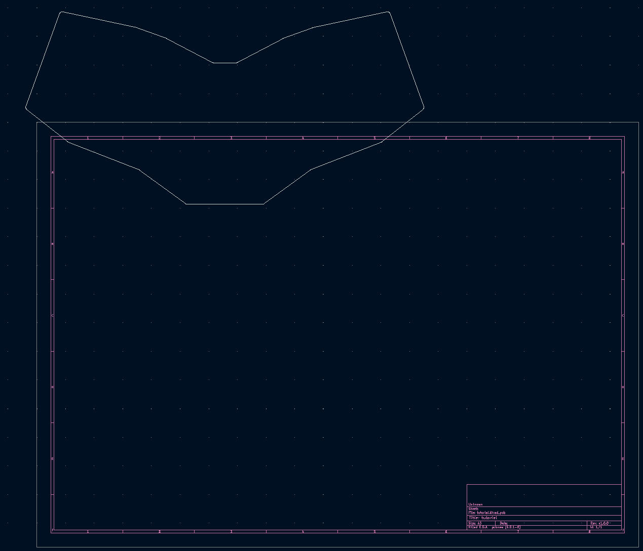
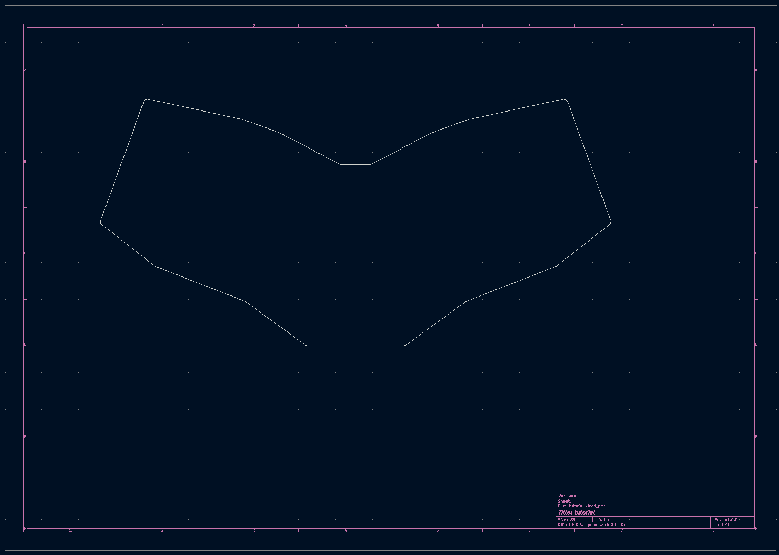
You'll also notice a different preview here. We've transitioned from Ergogen's web preview into KiCad. (KiCAD 7 came out while this series was being written. These screenshots are of KiCAD 6, but there shouldn't be any significant difference.) You can still use the web version of Ergogen to generate these files if you'd like. Just be aware you actually need to start clicking the "Generate" button instead of waiting for the preview to automatically re-render.
One oddity here is that our PCB outline is way outside of KiCAD's default sheet. We can fix this with a quick tweak in the Points section.
units: ...
points:
  zones:
    matrix:
      # Fix placement on KiCAD sheet.
      anchor:
        shift: [100, -100]
      ...
outlines: ...
pcbs:
  tutorial:
    outlines:
      main:
        outline: board
That was simple enough. But our board's still completely unpopulated. In the earlier parts of this guide we defined where each key switch was going to go, but we haven't defined the actual switches themselves yet. In KiCAD terms, we need to define the "Footprint" of the switches.
units: ...
points: ...
outlines: ...
pcbs:
  tutorial:
    outlines:
      main:
        outline: board
    footprints:
      choc_hotswap:
        what: choc
        where: true
        params:
          keycaps: true
          reverse: false
          hotswap: true
          from: "{{column_net}}"
          to: "{{colrow}}"
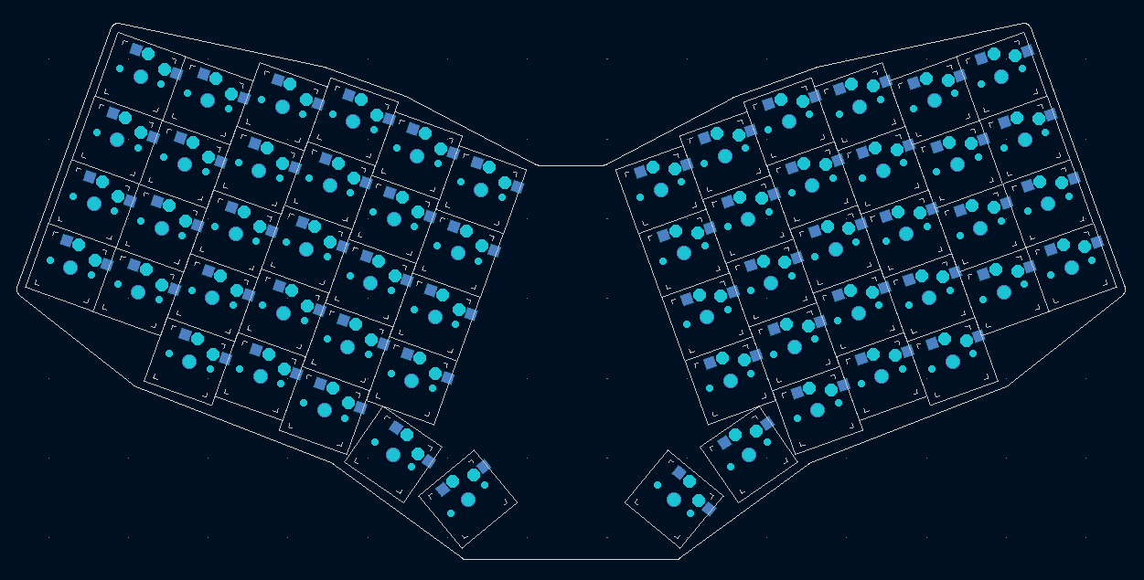
Now it's starting to look like a PCB! There's a lot going on here. Let's break down everything we just added. The footprints: section is naturally where we're going to add our part footprint definitions.
The first footprint we're going to define will be for the key switches themselves. We're leveraging Choc v1 switches in this design, and are going to be supporting "hotswap" sockets, so we've given it the creative name of choc_hotswap:.
The what: property specifies which footprint we're using. The Ergogen GitHub repository has a list of the default available footprints. We want to use the choc.js footprint, so these switch footprints are set as what: choc. The where: property allows us to specify where this footprint should apply. Ergogen has a tagging property we haven't touched on before, allowing you to flag certain keys to get certain footprints or properties applied to them. This could allow you to create some pretty unusual designs, hypothetically letting us set up MX switches for the main keys and Choc switches for the thumbs, etc. This board is using the same footprint for every key, so we're just going to use where: true.
In the params: section, we can adjust various settings of the footprint. If you open up the GitHub repository's choc.js file, you can see a list of available parameters at the top of the file. The keycaps: true property shows a box outline around the edges of where a 1u Choc keycap would be fit. The reverse: false property allows us to specify if we want the footprint to appear on the top and bottom of a PCB. This is a single-side unibody design, so we've set this to false. Finally, hotswap: true specifies that we'd like to use the hotswap socket footprint instead of the through-hole switch design.
At the end of the footprint we've got the from: and to: properties. These control the "Nets" of the PCB. It's a larger topic that we'll cover in a bit, but we're adding them now so Ergogen doesn't throw any errors.
units: ...
points: ...
outlines: ...
pcbs:
tutorial:
outlines:
main:
outline: board
footprints:
choc_hotswap:
what: choc
where: true
params:
keycaps: true
reverse: false
hotswap: true
from: "{{column_net}}"
to: "{{colrow}}"
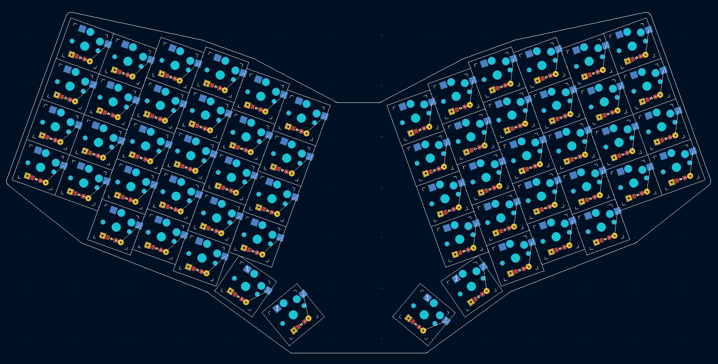
diode:
what: diode
where: true
params:
from: "{{colrow}}"
to: "{{row_net}}"
adjust:
shift: [0, -5]
Next we need to define the diodes used in our keyboard matrix. We've set up another entry in the footprints: section, cleverly named diode:. This footprint contains what: diode to refer to Ergogen's diode.js file. This footprint supports both surface mount smd diodes as well as through hole diodes, and doesn't have any parameters other than those mysterious from: and to: attributes. We have made one other adjustment however.
The where: true attribute places this diode footprint at the center of every point on our keyboard. This worked well for our choc footprints, but we don't want the diodes to be literally right on top of the key switch. Adding adjust.shift: [0, -5] moves the diode down beneath the key footprint.
Now that we've got our keys and our diodes set, let's do a very ham-fisted approach of trying to place the Arduino Pro Micro.
units: ...
points: ...
outlines: ...
pcbs:
tutorial:
outlines:
main:
outline: board
footprints:
choc_hotswap: ...
diode: ...
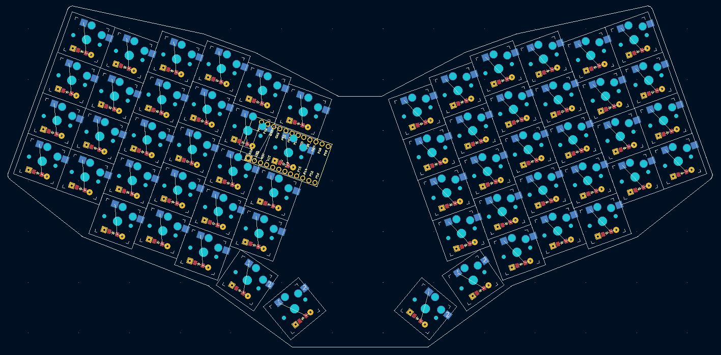
promicro:
what: promicro
params:
orientation: "down"
where:
ref: matrix_inner_top
shift: [0,0]
rotate: 0
You're starting to see a trend here. We've named our microcontroller's footprint promicro:, and the what: is a reference to promicro.js. The orientation: "down" parameter specifies whether or not the pinout for the Arduino should be with the microcontroller facing "up" or "down". Arduino Pro Micros aren't symmetrical, so you need to pick how you'd like it to be oriented. Most header pins are tall enough that they can fit the USB port in either configuration, so boards commonly use a face-down configuration for aesthetic reasons and to give the OLED screen something flush to sit against.
For the placement in where:, I set the reference to the matrix_inner_top key on the left side of the keyboard. It's one of the closer keys to the center of the board. From here we could try to shift: the key closer to the center, and give it a rotate: so that its pointing up instead of aligned with matrix_inner_top, but there's a new method we can use here.
units: ...
points: ...
outlines: ...
pcbs:
  tutorial:
    outlines:
      main:
        outline: board
    footprints:
      choc_hotswap: ...
      diode: ...
      promicro:
        what: promicro
        params:
          orientation: "down"
        where:
          ref.aggregate.parts: [matrix_inner_top, mirror_matrix_inner_top]
          shift: [0,0]
          rotate: 0
The ref.aggregate.parts: method allows you to specify location between two points. In this case, I specified a reference location between the matrix_inner_top left on the left, and the mirror_matrix_inner_top key on the right. Earlier versions of Ergogen would have just used ref: [matrix_inner_top, mirror_matrix_inner_top], but v4 makes things a bit more explicit what's going on.
units: ...
points: ...
outlines: ...
pcbs:
  tutorial:
    outlines:
      main:
        outline: board
    footprints:
      choc_hotswap: ...
      diode: ...
      promicro:
        what: promicro
        params:
          orientation: "down"
        where:
          ref.aggregate.parts: [matrix_inner_top, mirror_matrix_inner_top]
          shift: [0,0]
          rotate: -90
One quick application of rotate: -90 later, and things are starting to look good. Surprisingly good actually.
Real talk. When I created Part 1 of this guide I had assumed I had spaced the two halves of the keyboard too far apart. The placement of this Arduino looks almost perfect. I was planning on demonstrating how you can always go back and adjust earlier properties like points.mirror.distance: 2.5kx later on while building your config. Just for demonstration purposes, let's see if we can't make a better use of this space. Or at least arbitrarily different use.
units: ...
points:
zones:
matrix: ...
thumbs: ...
rotate: ...
mirror: &mirror
ref: matrix_inner_num
distance: 2kx
outlines:
raw: ...
keys: ...
board:
- what: polygon
operation: stack
points:
- ref: matrix_outer_num
shift: [-0.5px,0.5py]
- ref: matrix_ring_num
shift: [-0.5px,0.5py]
- ref: matrix_middle_num
shift: [-0.5px,0.5py]
- ref: matrix_middle_num
shift: [0.5px,0.5py]
- ref: matrix_inner_num
shift: [0.5px,0.5py]
- ref: matrix_inner_top
shift: [0.5px,0.5py]
- ref: mirror_matrix_inner_top
shift: [0.5px,0.5py]
- ref: mirror_matrix_inner_num
shift: [0.5px,0.5py]
- ref: mirror_matrix_middle_num
shift: [0.5px,0.5py]
- ref: mirror_matrix_middle_num
shift: [-0.5px,0.5py]
- ref: mirror_matrix_ring_num
shift: [-0.5px,0.5py]
- ref: mirror_matrix_outer_num
shift: [-0.5px,0.5py]
- ref: mirror_matrix_outer_bottom
shift: [-0.5px,-0.5py]
- ref: mirror_matrix_ring_mod
shift: [-0.5px,-0.5py]
- ref: mirror_thumbs_layer_cluster
shift: [-0.5px,-0.5py]
- ref: mirror_thumbs_space_cluster
shift: [-0.5py,-0.5px]
- ref: mirror_thumbs_space_cluster
shift: [0.5py,-0.5px]
- ref: thumbs_space_cluster
shift: [0.5py,-0.5px]
- ref: thumbs_space_cluster
shift: [-0.5py,-0.5px]
- ref: thumbs_layer_cluster
shift: [-0.5px,-0.5py]
- ref: matrix_ring_mod
shift: [-0.5px,-0.5py]
- ref: matrix_outer_bottom
shift: [-0.5px,-0.5py]
fillet: 2
combo: ...
pcbs:
tutorial:
outlines:
main:
outline: board
footprints:
choc_hotswap:
what: choc
where: true
params:
keycaps: true
reverse: false
hotswap: true
from: "{{colrow}}"
to: "{{col_net}}"
diode:
what: diode
where: true
params:
from: "{{colrow}}"
to: "{{row_net}}"
adjust:
shift: [0, -5]
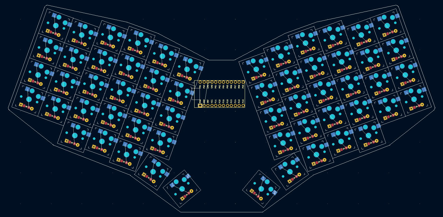
promicro:
what: promicro
params:
orientation: "down"
where:
ref.aggregate.parts: [matrix_inner_home, mirror_matrix_inner_home]
shift: [0,0]
rotate: -90
Alright, things are looking a bit more snug now! I went ahead and updated the points.mirror.distance: value from 2.5kx to 2kx. The Pro Micro's anchor reference has also been updated to use matrix_inner_home and its mirrored counterpart instead of matrix_inner_top. Finally, I added four new points to our outline. The outline now drops down from matrix_inner_num to matrix_inner_top before jumping across to the mirrored half. Similarly, the thumb keys linger on the thumbs_space_cluster for two additional points that shifted up to the top of the switch.
This is a fairly arbitrary change, but it's useful to show that none of the design decisions are set in stone. It's also important to remember that you pay per square inch when fabricating a PCB, so these sorts of small improvements can add up over time.
units: ...
points:
  zones:
    matrix: ...
    thumbs: ...
  rotate: ...
  mirror: &mirror
    ref: matrix_inner_num
    distance: 2kx
outlines: ...
pcbs:
  tutorial:
    outlines:
      main:
        outline: board
    footprints:
      choc_hotswap: ...
      diode: ...
      promicro: ...
      oled:
        what: oled
        params:
          side: "F"
          SDA: P2
          SCL: P3
        where:
          ref.aggregate.parts: [matrix_inner_home, mirror_matrix_inner_home]
          shift: [-6,-19]
          rotate: 90
We're wrapping up the parts now. Next is the footprint for the OLED screen. The what: oled portion refers to oled.js, and the where: parameters should be starting to look a little familiar. This footprint has an awkward shift: [-6, -19] on it. For whatever reason, the anchor point for the footprint itself isn't centered on the screen's pins.
The params: section has a few attributes we haven't seen before. side: "F" specifies that we're dealing with the front of the OLED screen, but what's SDA: and SCL:? That's an excellent question. One I'm not going to answer just yet.
units: ...
points: ...
outlines: ...
pcbs:
  tutorial:
    outlines:
      main:
        outline: board
    footprints:
      choc_hotswap: ...
      diode: ...
      promicro: ...
      oled: ...
      reset:
        what: button
        params:
          from: GND
          to: RST
        where:
          ref.aggregate.parts: [matrix_index_mod, mirror_matrix_index_mod]
          shift: [0, -1]
          rotate: -90
The last component we're dealing with is a reset button for the microcontroller. This allows you to reset the Arduino Pro Micro and put it into a flashing state for applying new firmware. This footprint is defined by button.js, and we're once again seeing those unusual from: and to: parameters. Let's wrap up the PCB layout section and finally tackle what's going on with those net parameters.
It's worth noting that this is a pretty barebones PCB. It's a unibody design, so we didn't need to use trrs.js to define a headphone jack to connect the two sides of a split keyboard. We're also not using a Nice!Nano wireless microcontroller, so we don't need to worry about a lipo battery and its jstph.js battery header.
Casting a Net
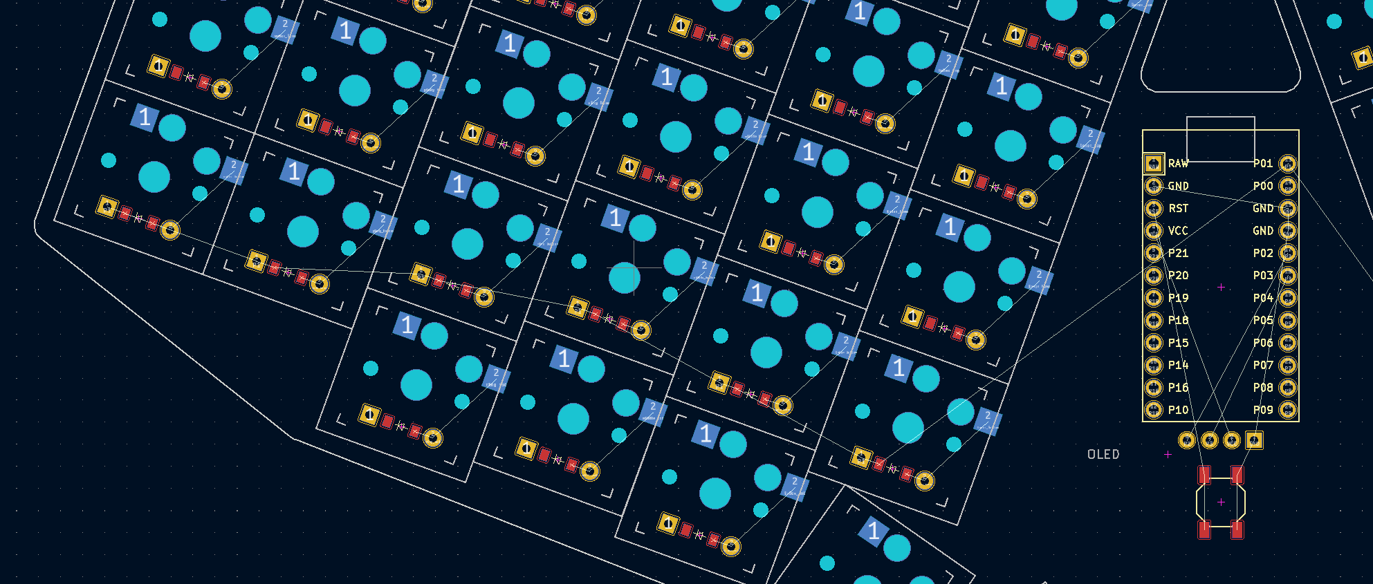
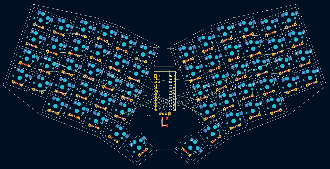
If you've been following along with this guide, you may have noticed some unusual things about the PCB file that Ergogen is creating. First of all: None of these parts are connected. There's just a blank void with several part footprints outlined by the edge of our board. Most PCBs you've looked at generally have thick lines connecting the parts together.
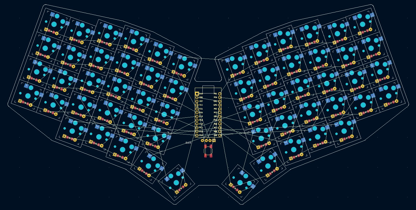
Furthermore, you may have noticed that when we placed the OLED screen and reset buttons, small thin white lines started appearing on our PCB. These don't look like normal PCB lines though. They're just shooting diagonal across the board between different pins. The clever ones among you may have started getting a sinking feeling when they noticed that the VCC pin on the OLED screen has a thin white line pointing to the VCC pin on the Arduino Pro Micro.
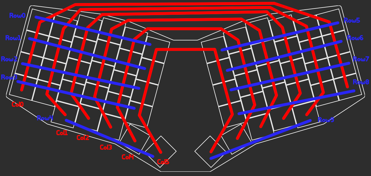
That's right. It's our job to make all of these connections. Welcome to the fun world of routing traces. A "trace" on a PCB is a small strip of metal connecting two parts on the board. It's similar to connecting components together with a jumper cable on a breadboard. The catch here is that the PCB only has two sides: A front and a bottom. I connected the VCC and GND pins with red traces on the front of the board, but needed to connect the P2 and P3 pins with blue traces on the backside of the board so they could pass under the red traces.
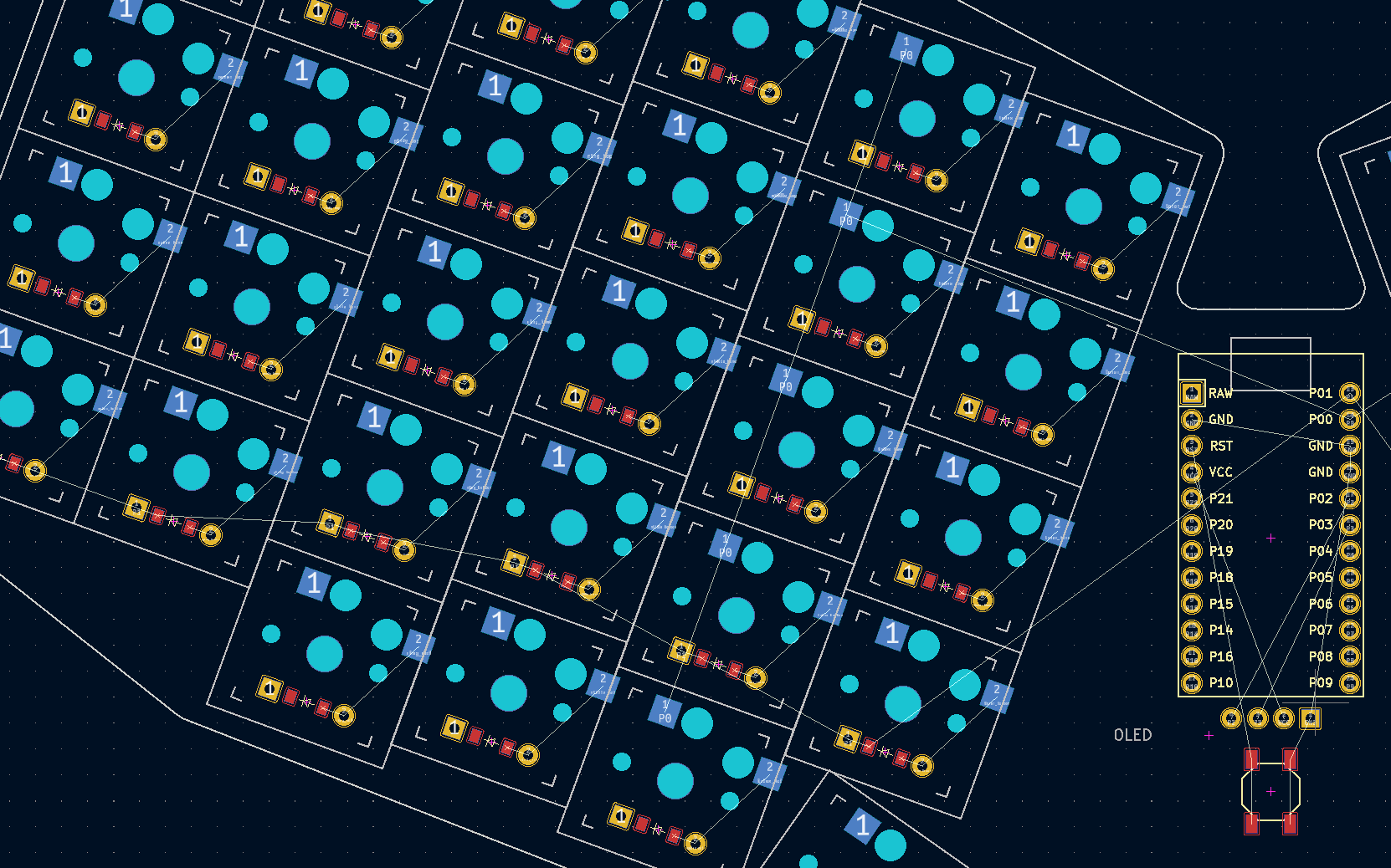
This is a manual and time consuming process. Worst yet, if you notice an error in your Ergogen config, you need to generate a new blank PCB and start all over again. Defining nets can help aid in this process considerably however. If we weren't able to specify that the OLED's left pin connected to the Arduino's 17th pin, we'd be left constantly flipping back and forth between part documentation, our schematics / config files, and the PCB itself. By defining in Ergogen which parts connect to one another, Ergogen can force us to wire things correctly.
When you're in the process of actively connecting two parts together, KiCAD will highlight the pins that your Ergogen config has specified that it would be alright for you to wire them to. You can see this behavior in this mid-routing screenshot where the two P2 pins are lit up like a Christmas tree.
So the next big step in our Ergogen config is defining all of these nets. We've seen a few of these definitions already in our file. Those from: and to: lines I skipped over earlier? We're finally getting back to those now.
The footprint file in Ergogen's Github repository defines the attribute name for a pin. from: and to: are conventions that footprint authors commonly use when a component only has two pins, but it's not a hard and fast rule.
params: {
  designator: 'B', // for Button
  side: 'F',
  from: undefined,
  to: undefined
}Here's the top section of the reset button we defined earlier. It has some metadata fields like designator: and side:, and then these undefined from: and to: fields. If we don't override the designator or the side it will use these defaults, but we have to define from: and to:
params: {
  designator: 'OLED',
  side: 'F',
  VCC: {type: 'net', value: 'VCC'},
  GND: {type: 'net', value: 'GND'},
  SDA: undefined,
  SCL: undefined
},Jumping back to the OLED footprint, we can see a slightly different configuration. The OLED screen on the keyboard needs power, and it also requires several pins to communicate with the Arduino. VCC is the term for regulated power coming from a microcontroller, and we also need a GND pin to complete the circuit. This OLED screen is powered by I2C serial communication which uses pins commonly defined as SDA and SCL.
Rather than arbitrarily coming up with new names for these pins, this footprint users the industry standard. VCC and GND are such common abbreviations that the footprint goes ahead and defines those pins for us. It doesn't know which SDA and SCL pins we'd like to use however, so we still need to define those.
In our Ergogen config, we referenced this OLED footprint with SDA: P2 and SCL: P3. This tells Ergogen, "If you see anything with a P2 pin on it, then this OLED screen's SDA pin is okay to connect to it. Our Arduino Pro Micro footprint has such a P2 pin, so lets look at its definition now.
  params: {
    designator: 'MCU',
    orientation: 'down',
    RAW: {type: 'net', value: 'RAW'},
    GND: {type: 'net', value: 'GND'},
    RST: {type: 'net', value: 'RST'},
    VCC: {type: 'net', value: 'VCC'},
    P21: {type: 'net', value: 'P21'},
    P20: {type: 'net', value: 'P20'},
    P19: {type: 'net', value: 'P19'},
    P18: {type: 'net', value: 'P18'},
    P15: {type: 'net', value: 'P15'},
    P14: {type: 'net', value: 'P14'},
    P16: {type: 'net', value: 'P16'},
    P10: {type: 'net', value: 'P10'},
    P1: {type: 'net', value: 'P1'},
    P0: {type: 'net', value: 'P0'},
    P2: {type: 'net', value: 'P2'},
    P3: {type: 'net', value: 'P3'},
    P4: {type: 'net', value: 'P4'},
    P5: {type: 'net', value: 'P5'},
    P6: {type: 'net', value: 'P6'},
    P7: {type: 'net', value: 'P7'},
    P8: {type: 'net', value: 'P8'},
    P9: {type: 'net', value: 'P9'}
}Woah! That's a lot of pins! You can see all of these pins are predefined here. For our OLED screen, the VCC pin automatically matched up with the Arduino's VCC pin since they were defined to the exact same value. In the case of the data pins, the SDA: P2 pin has a thin white line leading to the Arduino Pro Micro because we defined it as such.
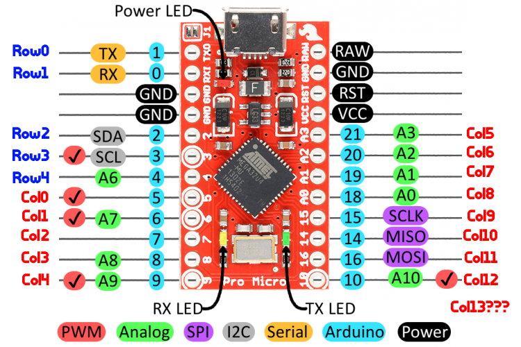
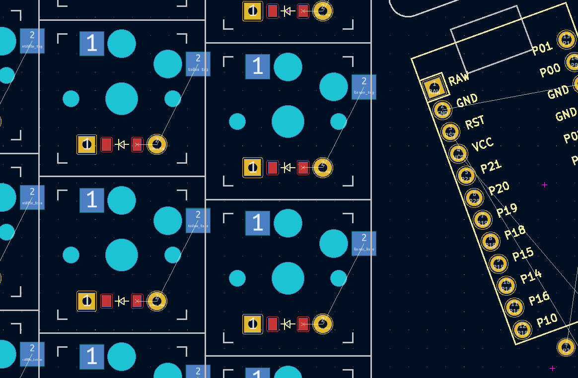
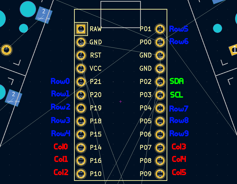
The P1-P21 pins seem a little generic at first, but let's go back and take a look at the Arduino screenshot and our Pro Micro footprint.

The Arduino footprint is oriented face down, so you need to mentally mirror these two diagrams. Once you do that however, you can see the same pattern of RAW, GND, RST, VCC, 21, 20, 19, etc. Pin numbers are a tricky thing on Arduinos. The ATmega32U4 processor has its own internal pin numbering, and on top of that pins can have multiple definitions. 2 is also the SDA pin, and 21 is also the A3 analog pin. In general however, most Arduino-based projects will discuss their wiring in terms of "Arduino" pins, or sometimes "Digital" pins. That's what this footprint has done here. They've just tacked P for "Pin" in front. (These pin names are also treated as a text string. P9 and P09 are considered two different pin labels, so don't go adding leading zeroes to your pin config.)
So at this point we understand how footprint nets are defined, and we've seen it in action on the few small footprints that we've added. We still don't have any nets going from our key switches to the Arduino however. Let's back up a minute and look at the existing key and diode definitions.
pcbs:
  tutorial:
    outlines:
      main:
        outline: board
    footprints:
      choc_hotswap:
        what: choc
        where: true
        params:
          keycaps: true
          reverse: false
          hotswap: true
          from: "{{column_net}}"
          to: "{{colrow}}"
      diode:
        what: diode
         where: true
        params:
          from: "{{colrow}}"
          to: "{{row_net}}"
        adjust:
          shift: [0, -5]
These footprints have had from: and to: definitions this entire time, and sure enough, you can see some nets in between the switch and the diode at every key.
The choc_hotswap: and diode: sections are using a new syntax we haven't seen yet. The from: "{{colrow}}", to: "{{col_net}}", and to: "{{row_net}}" properties have introduced curly brackets to our config file. (If you're looking at older Ergogen v3 configs, you'll instead see from: =colrow with an equal sign instead.)
This curly bracket syntax allows us to set "key-level attributes". Unlike the OLED screen on the Reset button footprints, we don't want to just straight wire every key on our keyboard to GND or VCC. We need to build out the matrix, and these key-level attributes are part of that.
In the next step of this guide, we'll be running those column and row lines we outlined back in the matrix section. The row lines will connect to one side of our switch, and the column lines will connect to the other side of the switch. It would be nice and simple, but we've also got the diodes to hook up.
The from: {{colrow}} parameter inside of choc_hotswap: and diode: signal to Ergogen that every key's switch needs to be wired up to every key's diode. They share this internal wiring because they both use {{colrow}} as a key-level net name.
The other properties are another one of those slightly confusing community naming convention vs. fixed Ergogen property name topics. The col_net and row_net (or sometimes column_net and row_net) properties you frequently see online in other people's Ergogen configs are just inherited from the original Absolem days. col_net and row_net are just popular conventions. colrow on the other hand is a function built into Ergogen. It's an aliased variable to the column-row intersection at that particular key.
All you really need to know here is that this is the portion of our code responsible for wiring up the diodes at each key. As long as you stay consistent in your use of col_row, row_net, and colrow you should be fine. Let's finally move on to creating our matrix.
(It's probably also worth pointing out at this point that our diode footprint has both options for through hole and surface mount device footprints. You can use a diode with legs that need to be soldered through the holes, or smaller smd diodes that only need to be soldered onto the pads. For reasons we'll cover later, having at least one pair of through hole components on this board helps us out a bit. If you're wondering why a pair of pads are connected so closely with those small through holes, there's your explanation.)
units: ...
points:
  zones:
    matrix:
      anchor: ...
      key: ...
      columns:
        outer: ...
        pinky: ...
        ring: ...
        middle: ...
        index: ...
        inner: ...
      rows:
        mod: ...
        bottom:
          row_net: P1
        home: ...
        top: ...
        num: ...
    thumbs:
      key: ...
      anchor: ...
      columns:
        layer: ...
        space: ...
      rows:
        cluster: ...
  rotate: -20
  mirror: ...
outlines: ...
pcbs: ...
Wiring up our keyboard matrix's nets requires us to go all the way back up into the points: section of our config. I've hidden most of the properties we added during Part 1, but you can see the newly added bottom.row_net: P1 attribute.
This does pretty much what you expect. You can see a net coming from the Arduino's P1 pin connecting to all of the keys in the bottom row.
units: ...
points:
  zones:
    matrix:
      anchor: ...
      key: ...
      columns:
        outer: ...
        pinky: ...
        ring: ...
        middle: ...
        index:
          key:
            stagger: -2.5
            column_net: P0
        inner: ...
      rows:
        mod: ...
        bottom:
          row_net: P1
        home: ...
        top: ...
        num: ...
    thumbs:
      key: ...
      anchor: ...
      columns:
        layer: ...
        space: ...
      rows:
        cluster: ...
  rotate: -20
  mirror: ...
outlines: ...
pcbs: ...
The column_net: property works the exact same way, just for columns instead of rows. Just note that you need to put it inside of the key: property of each column.
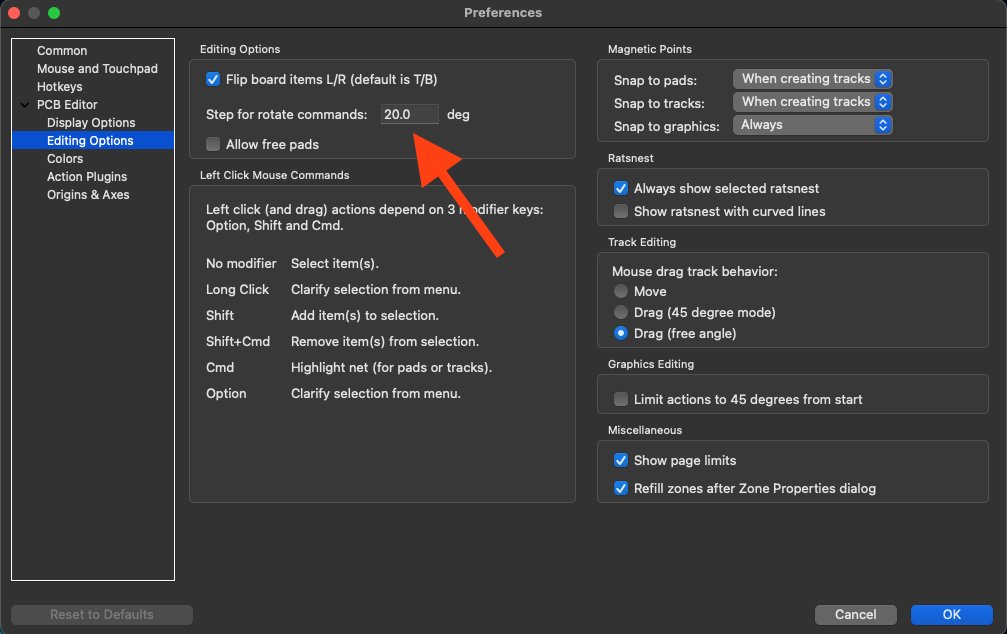
Before we continue, mosey on over to the Editing Options section of your KiCAD Settings. There's an option for Step for rotate commands:. Change that to match whatever rotate: attribute to inside of the points: section. In our case, 20 deg.
Now if you go back to your KiCAD window, you can select the entire board with Ctrl/Cmd-a, and rotate the two halves back and forth with r and Shift-r.
Ah, that feels better.
This tutorial isn't going to be a full KiCAD guide. Thankfully you don't need to get deep into this software in order to make a keyboard. KiCAD actions are very "modal", and are usually triggered by discrete clicks or key commands. Unlike a drawing application like Paint or Photoshop, you create traces by clicking where you want to start drawing a line, dragging the line to where it needs to go, and then clicking a second time to stop drawing.
Let's go ahead and wire up our row now.
Here's our row.
And here's our column. (Shout out to my CMS stretching the image out a bit.)
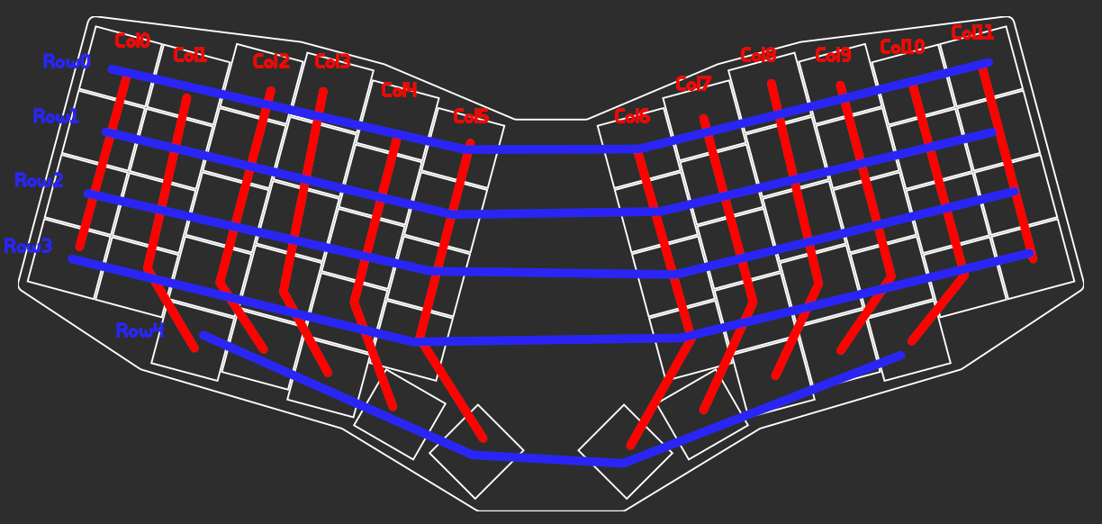
Oof. I did not think through which pins I used for these columns and rows, huh? Those row and column traces are having to reach over to the far side of the keyboard in order to get hooked up. Let's see if we can more intelligently map out these pins.
units: ...
points:
  zones:
    matrix:
      anchor: ...
      key: ...
      columns:
        outer:
          rows.mod.skip: true
          key.column_net: P14
        pinky:
          rows.mod.skip: true
          key.column_net: P16
        ring:
          key:
            stagger: 5
            column_net: P10
        middle:
          key:
            stagger: 2.5
            column_net: P7
        index:
          key:
            stagger: -2.5
            column_net: P8
        inner:
          rows.mod.skip: true
          key:
            stagger: -2.5
            column_net: P9
      rows:
        mod:
          row_net: P15
        bottom:
          row_net: P18
        home:
          row_net: P19
        top:
          row_net: P20
        num:
          row_net: P21
    thumbs:
      key: ...
      anchor: ...
      columns:
        layer: ...
        space: ...
      rows:
        cluster: ...
  rotate: -20
  mirror: ...
outlines: ...
pcbs: ...
We are almost there. We've set all of the column nets, but we still need to define the row nets for the right side of the keyboard. Thankfully, Ergogen provides a syntax to specifically target mirrored sections of the board.
rows:
  mod:
    row_net: P15
    mirror.row_net: P6
  bottom:
    row_net: P18
    mirror.row_net: P5
  home:
    row_net: P19
    mirror.row_net: P4
  top:
    row_net: P20
    mirror.row_net: P0
  num:
    row_net: P21
    mirror.row_net: P1
There we go! All of our nets are now set up!
Except wait, the thumbs aren't connected to anything. Right, we were going to nudge all of those net definitions over by one. Let's clean that up real quick. Key level overrides to the rescue!
units: ...
points:
  zones:
    matrix:
      anchor: ...
      key: ...
      columns:
        outer:
          rows.mod.skip: true
          key.column_net: P14
        pinky:
          rows.mod.skip: true
          key.column_net: P16
        ring:
          key:
            stagger: 5
            column_net: P10
          rows.mod.column_net: P16
        middle:
          key:
            stagger: 2.5
            column_net: P7
          rows.mod.column_net: P10
        index:
          key:
            stagger: -2.5
            column_net: P8
          rows.mod.column_net: P7
        inner:
          rows.mod.skip: true
          key:
            stagger: -2.5
            column_net: P9
      rows:
        mod:
          row_net: P15
          mirror.row_net: P6
        bottom:
          row_net: P18
          mirror.row_net: P5
        home:
          row_net: P19
          mirror.row_net: P4
        top:
          row_net: P20
          mirror.row_net: P0
        num:
          row_net: P21
          mirror.row_net: P1
    thumbs:
      key: ...
      anchor: ...
      columns:
        layer:
          key:
            splay: -15
            column_net: P8
        space:
          key:
            width: 1.5kx
            splay: 75
            shift: [2.5,-3.25]
            column_net: P9
      rows:
        cluster:
          row_net: P15
          mirror.row_net: P6
  rotate: -20
  mirror: ...
outlines: ...
pcbs: ...
In this step we finished wiring up our thumb keys, and we also included some row level overrides in our column definitions. The rows.mod.column_net: P16 inside of column.ring: tells Ergogen that we want to override the rest of that column's column_net: P10 for just the mod key.
With that, we're finally done. There was a lot of theory talk here when it came to the nets, but our PCB configuration is finished!
End of Part 3
units:
  # Proxy Spacing Variables
  kx: cx
  ky: cy
  # Padding Variables
  px: kx + 4
  py: ky + 4
points:
  zones:
    # The primary 6x4 key matrix, plus 3 modifiers.
    matrix:
      # Position in center of KiCAD workspace.
      anchor:
        shift: [100, -100]
      # Choc spacing
      key:
        padding: 1ky
        spread: 1kx
      columns:
        # Hide the first two mods and the last mod.
        # Provide a Sofle-like column stagger.
        outer:
          rows.mod.skip: true
          key.column_net: P14
        pinky:
          rows.mod.skip: true
          key.column_net: P16
        ring:
          key:
            stagger: 5
            column_net: P10
          rows.mod.column_net: P16
        middle:
          key:
            stagger: 2.5
            column_net: P7
          rows.mod.column_net: P10
        index:
          key:
            stagger: -2.5
            column_net: P8
          rows.mod.column_net: P7
        inner:
          rows.mod.skip: true
          key:
            stagger: -2.5
            column_net: P9
      rows:
        # Four main rows, one partial row.
        mod:
          row_net: P15
          mirror.row_net: P6
        bottom:
          row_net: P18
          mirror.row_net: P5
        home:
          row_net: P19
          mirror.row_net: P4
        top:
          row_net: P20
          mirror.row_net: P0
        num:
          row_net: P21
          mirror.row_net: P1
    # Thumb cluster for Layer and Space keys.
    thumbs:
      # Choc spacing
      key:
        padding: 1ky
        spread: 1kx
      # Place thumbs where the inner mod would go.
      anchor:
        ref: matrix_inner_mod
        shift: [2, -2]
      columns:
        # Fan thumbs out by -15 degrees.
        layer:
          key:
            splay: -15
            column_net: P8
        # Spacebar uses a 1.5 wide key.
        space:
          key:
            width: 1.5kx
            splay: 75
            shift: [2.5,-3.25]
            column_net: P9
      rows:
        # Thumbs only have one row.
        cluster:
          row_net: P15
          mirror.row_net: P6
  # Mirror keyboard halves with a moderate rotation.
  rotate: -20
  mirror: &mirror
    ref: matrix_inner_num
    distance: 2kx
outlines:
  # Pure key outline.
  raw:
    - what: rectangle
      where: true
      size: [px, py]
  # Key outlines with 0.5mm removed to show key overlaps.
  keys:
    - what: rectangle
      where: true
      size: [kx-0.5,ky-0.5]
  # PCB board outline.
  board:
    - what: polygon
      operation: stack
      points:
        - ref: matrix_outer_num
          shift: [-0.5px,0.5py]
        - ref: matrix_ring_num
          shift: [-0.5px,0.5py]
        - ref: matrix_middle_num
          shift: [-0.5px,0.5py]
        - ref: matrix_middle_num
          shift: [0.5px,0.5py]
        - ref: matrix_inner_num
          shift: [0.5px,0.5py]
        - ref: matrix_inner_top
          shift: [0.5px,0.5py]
        - ref: mirror_matrix_inner_top
          shift: [0.5px,0.5py]
        - ref: mirror_matrix_inner_num
          shift: [0.5px,0.5py]
        - ref: mirror_matrix_middle_num
          shift: [0.5px,0.5py]
        - ref: mirror_matrix_middle_num
          shift: [-0.5px,0.5py]
        - ref: mirror_matrix_ring_num
          shift: [-0.5px,0.5py]
        - ref: mirror_matrix_outer_num
          shift: [-0.5px,0.5py]
        - ref: mirror_matrix_outer_bottom
          shift: [-0.5px,-0.5py]
        - ref: mirror_matrix_ring_mod
          shift: [-0.5px,-0.5py]
        - ref: mirror_thumbs_layer_cluster
          shift: [-0.5px,-0.5py]
        - ref: mirror_thumbs_space_cluster
          shift: [-0.5py,-0.5px]
        - ref: mirror_thumbs_space_cluster
          shift: [0.5py,-0.5px]
        - ref: thumbs_space_cluster
          shift: [0.5py,-0.5px]
        - ref: thumbs_space_cluster
          shift: [-0.5py,-0.5px]
        - ref: thumbs_layer_cluster
          shift: [-0.5px,-0.5py]
        - ref: matrix_ring_mod
          shift: [-0.5px,-0.5py]
        - ref: matrix_outer_bottom
          shift: [-0.5px,-0.5py]
      fillet: 2
  # Combination preview showing outline and keys.
  combo:
    - name: board
    - operation: subtract
      name: keys
pcbs:
  tutorial:
    outlines:
      main:
        outline: board
    footprints:
      # Hotswap Choc keys.
      choc_hotswap:
        what: choc
        where: true
        params:
          keycaps: true
          reverse: false
          hotswap: true
          from: "{{column_net}}"
          to: "{{colrow}}"
      # Through Hole or SMD Diodes
      diode:
        what: diode
        where: true
        params:
          from: "{{colrow}}"
          to: "{{row_net}}"
        adjust:
          shift: [0, -5]
      # Face Down Arduino Pro Micro
      promicro:
        what: promicro
        params:
          orientation: "down"
        where:
          ref.aggregate.parts: [matrix_inner_home, mirror_matrix_inner_home]
          shift: [0,0]
          rotate: -90
      # OLED Screen
      oled:
        what: oled
        params:
          side: "F"
          SDA: P2
          SCL: P3
        where:
          ref.aggregate.parts: [matrix_inner_home, mirror_matrix_inner_home]
          shift: [-6,-19]
          rotate: 90
      # Four Pin Reset Button
      reset:
        what: button
        params:
          from: GND
          to: RST
        where:
          ref.aggregate.parts: [matrix_index_mod, mirror_matrix_index_mod]
          shift: [0, -1]
          rotate: -90
We still need to wire this bad boy together, but before we wrap up this PCB, I'd like to take a trip over to the Cases section and wrap up a few of the smaller Ergogen topics. When you're ready, head on over to Let's Design a Keyboard With Ergogen v4: Offline Ergogen, External Footprints, & Cases (Part 4)!