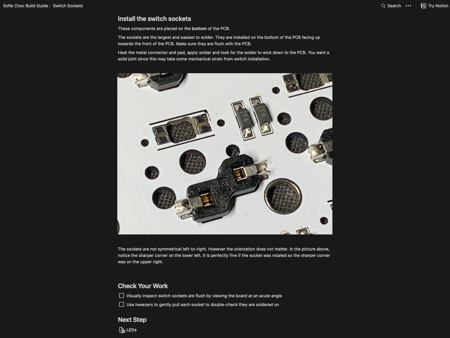
All good things must come to an end! We've come far since the introductory post! In Part 1 we created our keyboard's layout by leveraging points, in Part 2 we gave our board an outline, in Part 3 we discussed microcontrollers and created the basis for our PCB, and in Part 4 we imported external footprints and designed a keyboard case. We've reached the end of our journey with Ergogen.
The final steps of building a keyboard all take place outside of Ergogen. The biggest missing piece is actually creating the routes for our board in KiCAD. After that we need to create a custom firmware for the new keyboard, and finally there's the matter of actually sourcing the parts and assembling the keyboard.
This section is going to be a bit less click-by-click and line-by-line than the previous chapters. The remaining tools we need to leverage all have useful documentation and tutorials of their own, so the remainder of this guide is going to be giving some Ergogen-related tips and tutorial recommendations.
What a CAD!
The "CAD" in "KiCAD" comes from the term "Computer Aided Design". CAD itself is an offshoot of EDA, or Electronic Design Automation. This isn't just a stroll down memory lane (although fun fact, KiCAD is a portmanteau of the name of the lead developer's friend "Ki" and CAD), but it will hopefully be some useful context.
CAD software is old. Like, has its roots in the 1960s old. The most popular commercial CAD software today is EAGLE EDA. (I swear this series isn't a subtile plug for Autodesk, they've just acquired a ton of applications at this point.) If EAGLE's all-caps German acronym name wasn't enough of a hint, this app has been around for 35 years. It started off as a 16-bit DOS application.
This is all to say that CAD software, including KiCAD, has some very odd historical quirks. The conventions of this space were codified at a time when designers had arrow keys and trackballs. There's an unusually heavy reliance on hotkeys, and a "modality" you don't see in many modern apps.
CAD software is difficult to "feel" one's way around. Case in point, the simple act of drawing a line is unlike any image manipulation app you've ever worked with. Instead of clicking and dragging where you'd like to draw a trace, you click on a start point and then drag your mouse along the path where you'd like the trace to go. Once you've reached the final point, you click a second time exit the routing mode. It's a few steps removed from opening up Photoshop, clicking on the blurry-looking icon, and then clicking and dragging the blur tool around experimentally.

I cut my teeth on KiCAD with Brian Benchoff's excellent HackADay Creating A PCB In Everything series. It served as a general survey of various popular CAD softwares at the time, and walked readers through creating a KiCAD schematic (something we didn't need to do thanks to Ergogen creating our nets), designing a footprint from scratch (useful, but something that doesn't come up as often in the Ergogen community), and finally routing everything together (the last step we need to do here today).
Also, huh, a multi-part blog post with an introductory post that serves as a table of contents for the rest of the series. Maybe I learned more from Benchoff than just how CAD software works.At the time of writing this post, KiCAD 7 is hot off the presses. KiCAD goes through the usual incremental upgrades between versions, but any guide you find for KiCAD 4, 5, or 6 should still be somewhat useful to you. KiCAD 4 had some significant UI changes over KiCAD 3, but things have been much more subtile since then.
As far as additional resources go, KiCAD manages some recommendations themselves. This includes their own KiCAD Getting Started guide. Rene Poschl and Nate from Sparkfun also both have well regarded KiCAD 5 and KiCAD 4 guides. Ben Vallack also has a good keyboard-specific KiCAD video. Apologies for not having solid personal recommendations for more contemporary resources.
Routing Basics
Printed circuit boards are made out of an epoxy fiberglass composite known as FR-4. They're, you know, flat boards, and have a copper layer on each side to connect your components together. When working with PCBs, it's important to remember that you're dealing with a two sided object that has a defined front and back.
This isn't completely universal. You can save a dollar and get copper only one side of your board. You can also pay three times as much and get a four layer PCB that's a sandwich of multiple copper and FR-4 layers. In most situations however it's not worth saving a buck to deal with making a single layer board, and whatever issue is nudging you towards considering a four layer PCB can be likely be solved with some clever rearrangement of parts and traces. For the most part almost any PCB you design or interact with will be a two layer PCB.
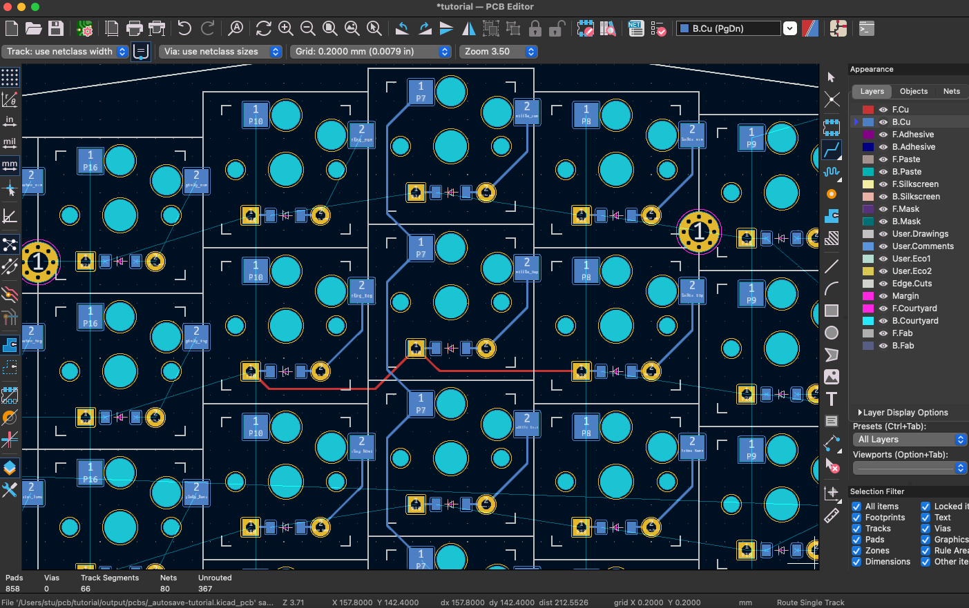
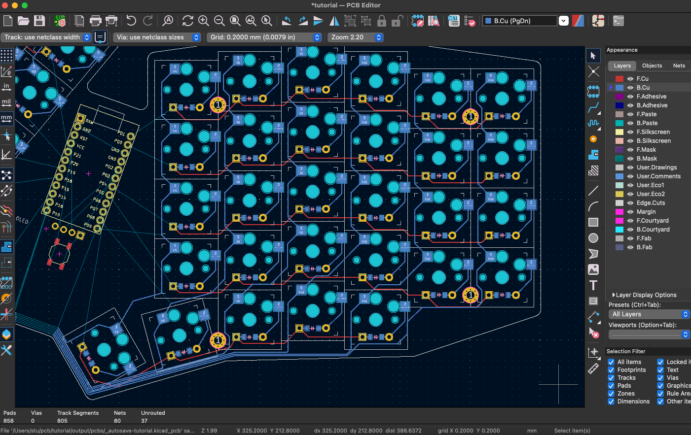
The copper line between two components on a PCB are known as a "Trace". The verb for defining a trace on your PCB is "Routing". Sometimes a trace will be referred to as a "Route". They're also occasionally known as "Tracks". The big last step we have in our keyboard design process is to route these traces on our empty PCB.
KiCAD draws traces on the front of the PCB as red lines. They're part of the F.Cu layer. (AKA "Front.Copper")
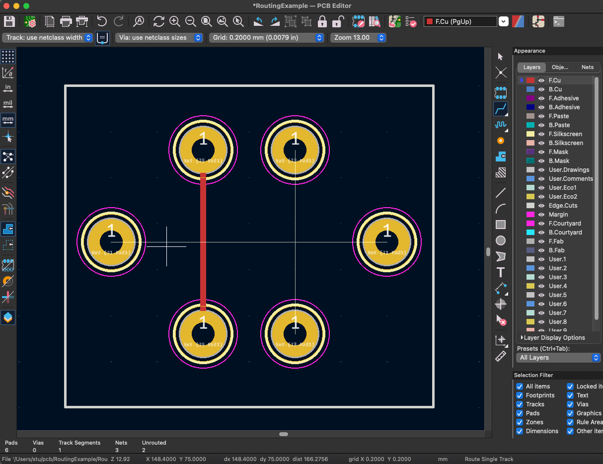
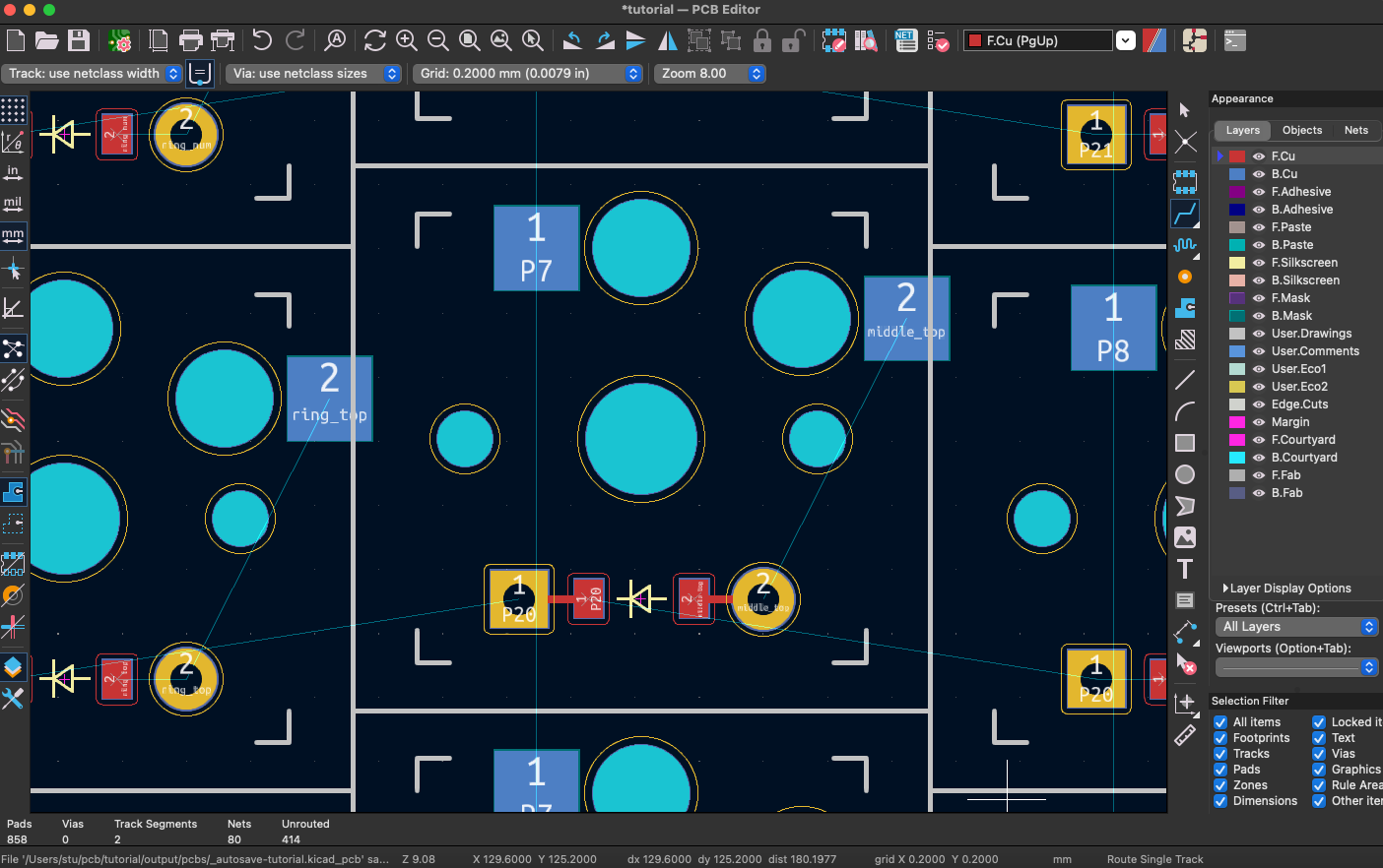
Traces on the back of the PCB are drawn in blue lines. They're part of the B.Cu layer. (AKA "Back.Copper".) In this primitive example, what would happen if we try to connect these two far left and far right pins together?
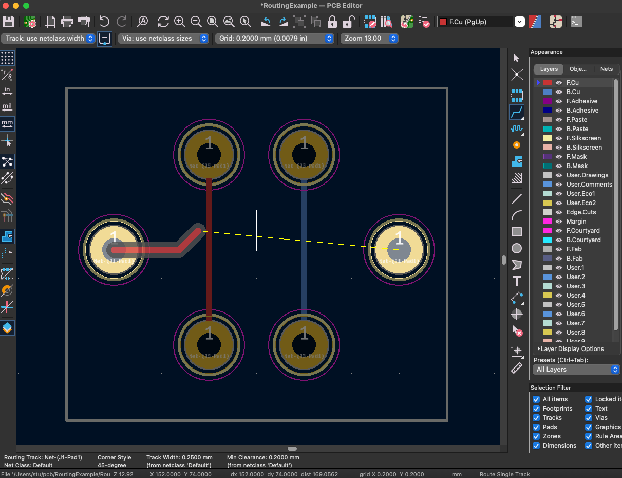
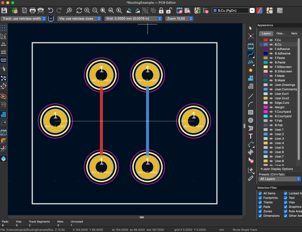
Our line gets stuck! KiCAD won't let us draw two red lines intersecting on top of one another. What if we switch to the B.Cu layer?
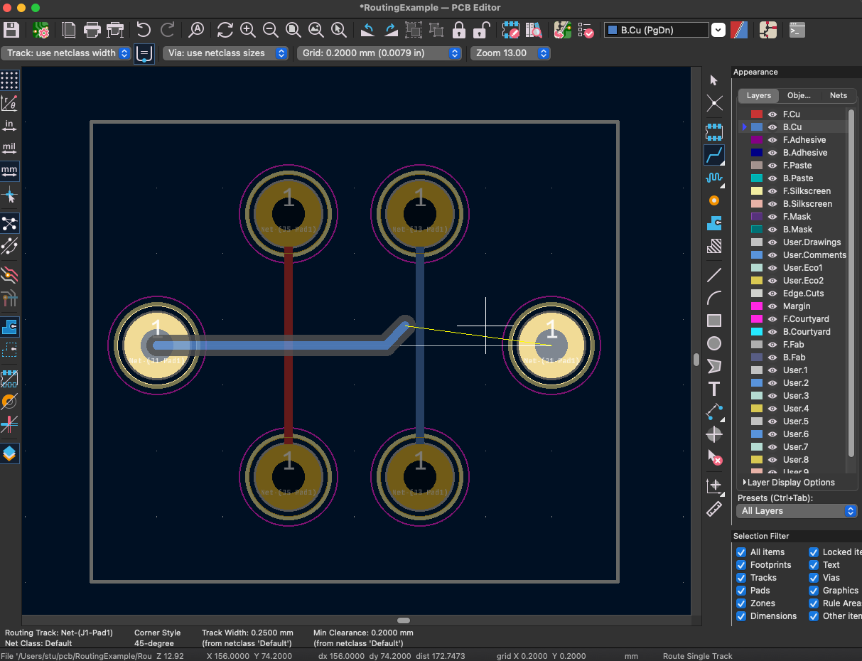
This time we managed to go over the F.Cu trace, but we got stuck again at the B.Cu trace.
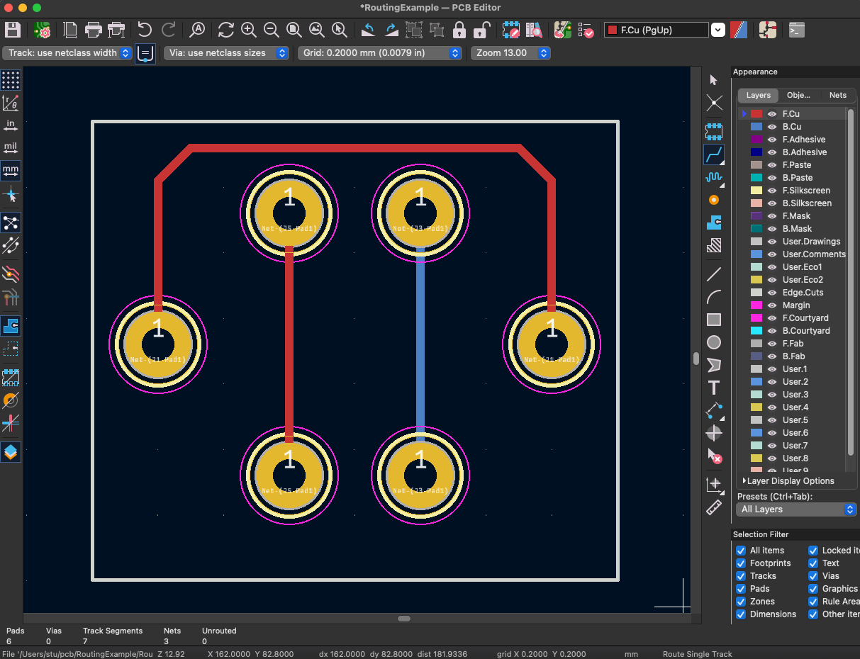
This isn't software. We can't just cheat across intersections. If you want to draw a front trace over another front trace... you can't. You need to go around. A big part of PCBs is getting smart about where you place components.
Sometimes we don't have the option of being smart however. If our board was a bit more narrow, we couldn't just sneak across the top. So what are we supposed to do in a situation like this?
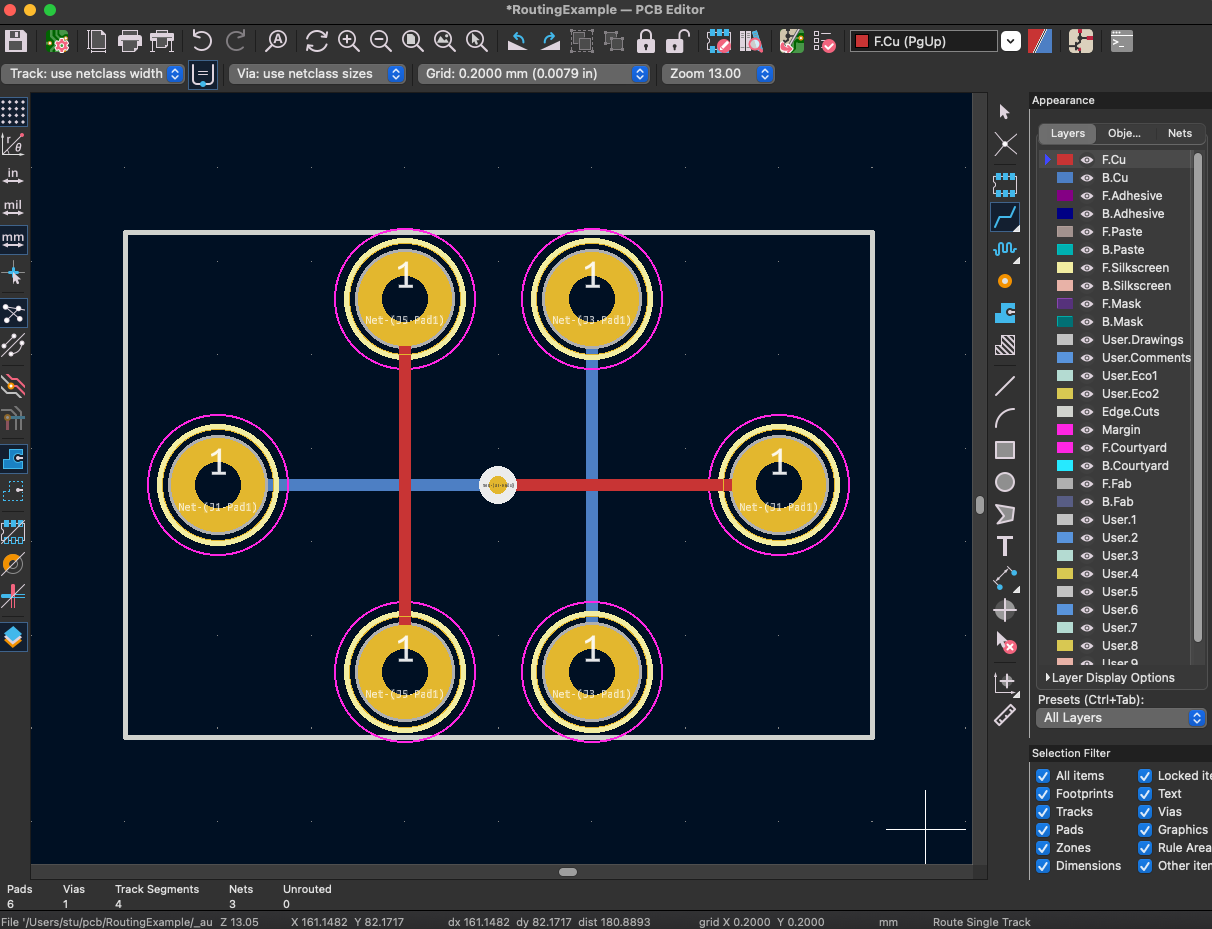
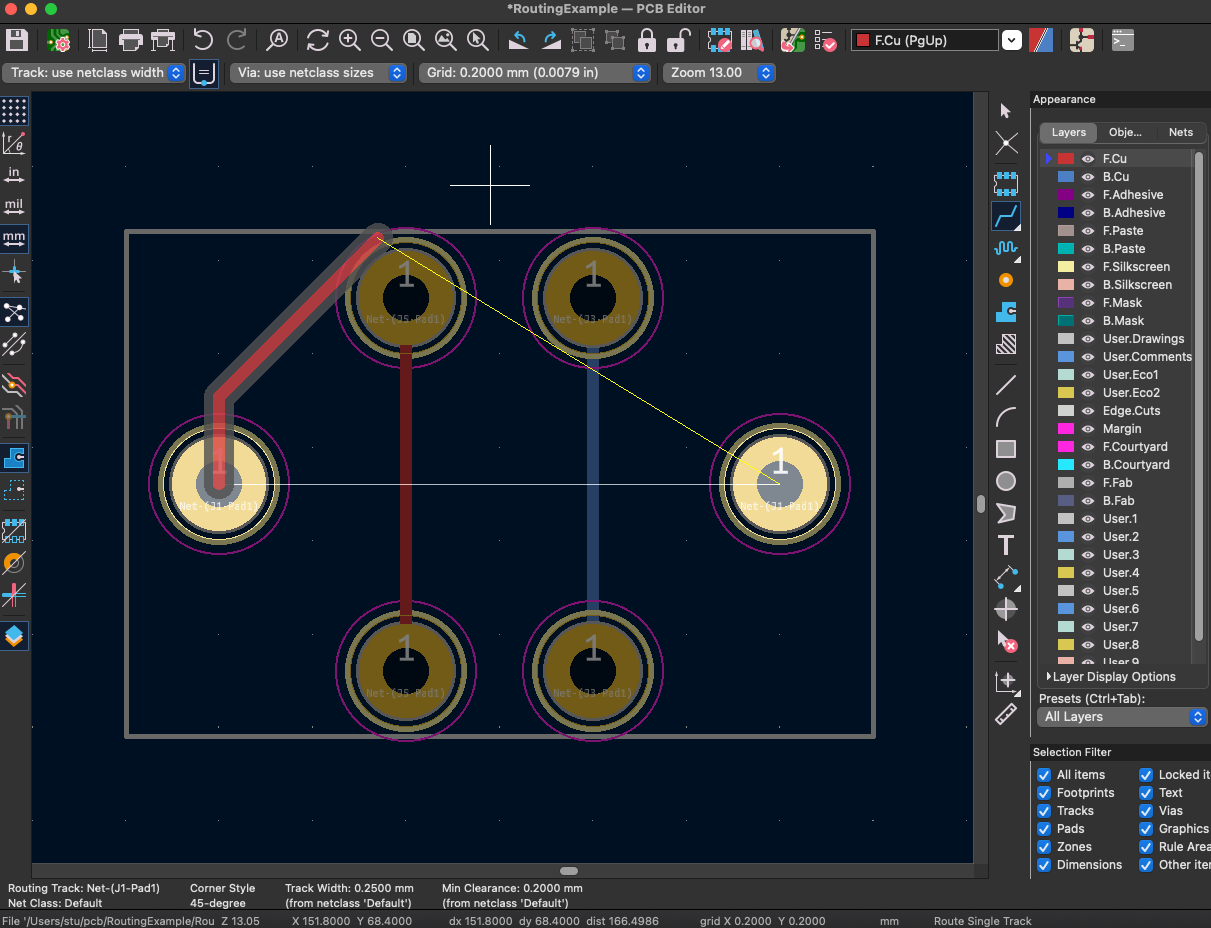
The one Get Out of Jail Free card we have when it comes to routing is the "Via". Vias are physical holes drilled in our PCB that allow traces to move from one side of the broad to the other. Sometimes our layout is just too complicated and there's no better way to get around an existing trace.
There's a variety of factors impacting the cost of a PCB. The primary cost comes from the side of the circuit board. You pay per square millimeter. The larger your keyboard, the more it's going to cost. Secondary to that is how long it takes to fabricate your keyboard. If the PCB manufacturer has to spend an inordinate amount of time working on your PCB, they'll usually charge you a bit extra. Vias are physically drilled into your PCB, and drilling takes time. It's usually a good idea to limit the number of Vias you use when designing a keyboard. If you need to use a dozen of them to get your microcontroller wired up, fine, but it's not something you really want to use on a per-key basis.
One last note on routing basics is the difference between "surface mount device" SMD pads and "through hole" pins. SMD pads are only exposed on one side of the board, so your trace needs to connect to it on the same side. In the above screenshot, our hotswap sockets need to connect to the blue pads on the back, while the reset button has red pads on the front. Through hole pins are physically drilled through a PCB and are exposed on both sides of the board. You can start your trace from either the front or the back when working with through holes components.
I'm generally a fan of SMD diodes for keyboards. They're a little more fiddly, but you don't have to worry about the trimmed through hole leads getting in the way of anything. SMD diodes are also shorter than the hotswap sockets we're working with, so they don't introduce any new design considerations there Despite all this, I kept the dual SMD and TH diode footprint on our example keyboard design. Having at least one through hole component on each key switch allows us to more easily hop back and forth from the front and back of the keyboard.
Routing A Keyboard
Enough theory! Let's route our keyboard. If you haven't already, download KiCAD and open the PCB file Ergogen created earlier. I had been using KiCAD 6 in all of the screenshots I had taken up till now, but I suppose I really should hop on the brand spanking new KiCAD 7. There shouldn't be too much that changed between the versions, but I don't want new users to get caught up on the names of settings and preferences if there's any small differences.
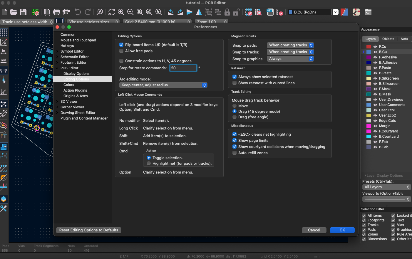
Speaking of which, let's start with a quick preference tweak. Navigate to File -> Settings, or press Cmd-, if you're on a Mac. Navigate to the Editing Options section. Change the "Step for rotate commands:" option from 90 degrees to whatever value you had set the rotate: value to your mirrored halves in your Ergogen config. In our case, that's 20 degrees.
Now if we tap the r or Shift-r key while working with a part, KiCAD will rotate it 20 degrees instead of 90 degrees. This is useful for pivoting between the different halves of the board and keeping all of our traces straight. To rotate the board, simply tap Cmd/Ctrl-a to select every component in your design, then r or Shift-r to rotate it.

My general approach when routing a board is to route the keyboard matrix and then figure out how to connect it to the microcontroller. To start with, let's figure out how we want to wire up an individual key.
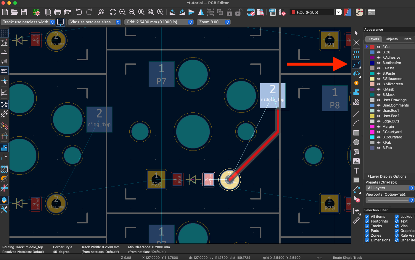
Hover your cursor over one of the through holes and press the x key to begin routing. You can also select the "Route Tracks" tool from the right side of KiCAD and click the pin or pad you want to start routing from. We've immediately run into a problem here though. Our track is on the red F.Cu layer, and we're trying to connect to a blue B.Cu pad.
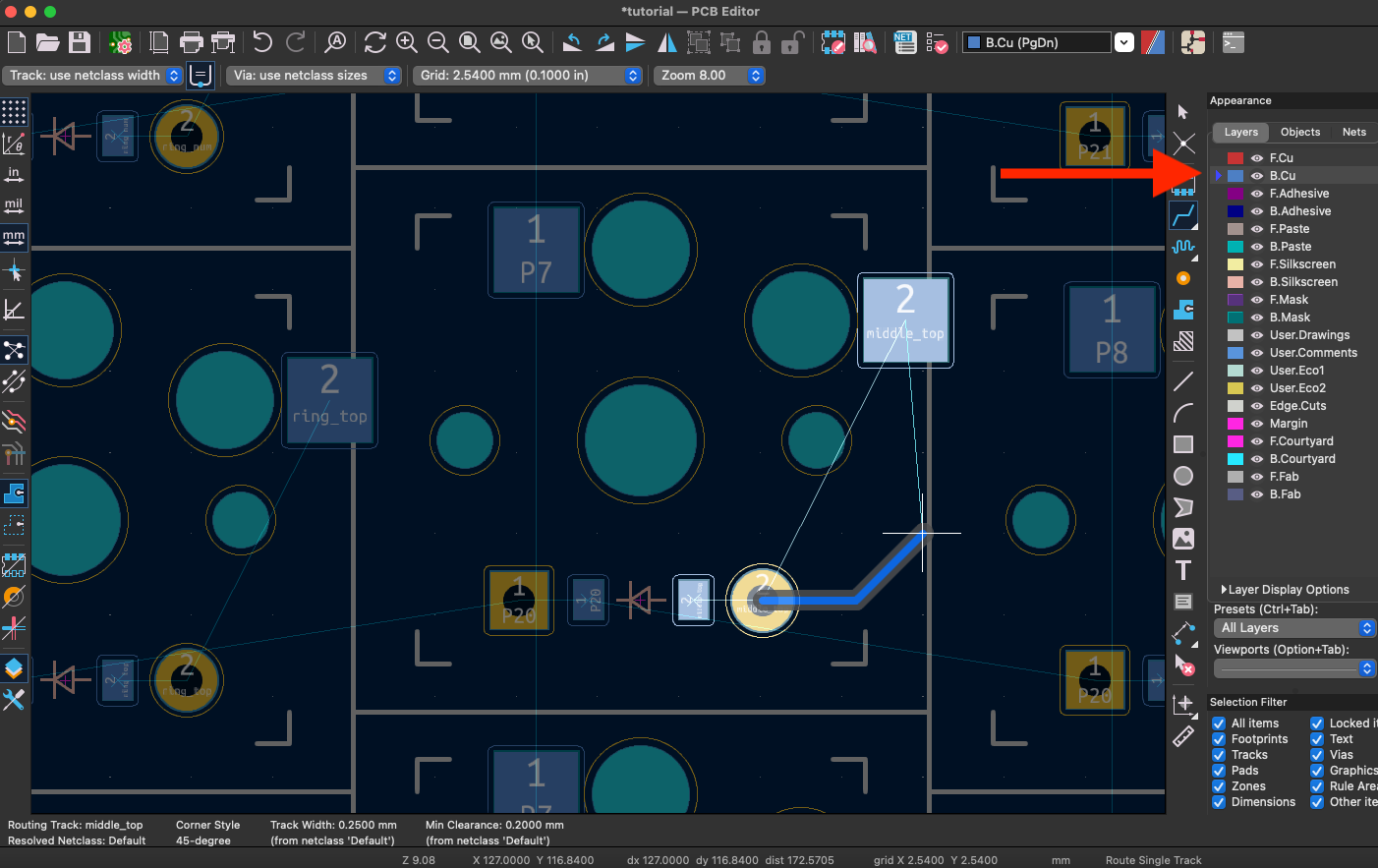
To switch sides of the board, tap the v key. You can also manually change front and back layers by using the panel on the right. Traces are always routed on the F.cu and B.cu layers, but you can use the other tools (lines, arcs, circles, text, etc.) to add elements to the other layers. Anything on the F.Silkscreen and B.Silkscreen layers will be drawn as a graphic on your board, and Edge.Cuts defines the physical edges of your PCB.
You may have noticed that your traces are really clunky. They're snapping to an almost absurdly large grid for the PCB we're working with. Let's fix that.
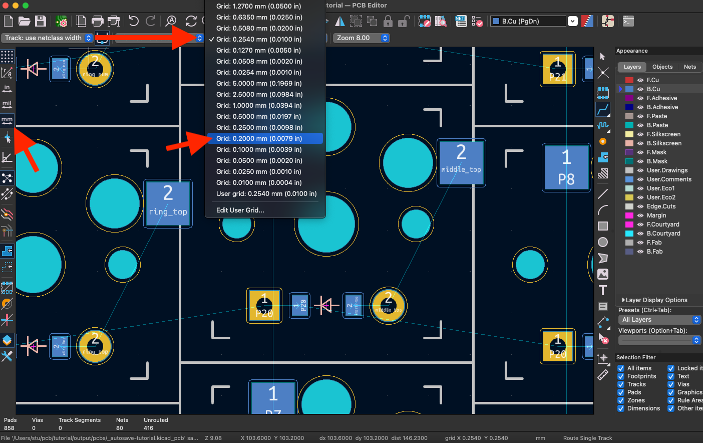
The Grid: drop down at the top of the page is defaulting to 0.2540mm. (In other words, 0.01 of an inch.) We need something considerably smaller. I personally like working with 0.2mm. It's small enough that you can flexibly route your board, but still on enough of a grid that aligning things doesn't become a nightmare. Feel free to experiment and see what works best for you.
Most of the measurements we're working with here make more sense in terms of millimeters. (Sorry my fellow Americans.) If KiCAD starts suddenly displaying property screens to you with five digit decimal inch measurements, you probably accidentally changed your units somewhere along the way. Thankfully you can quickly get back to millimeters by clicking the small "mm" icon on the left side of the screen.
Now that we're familiarized ourselves with KiCAD, onto the actual routing.
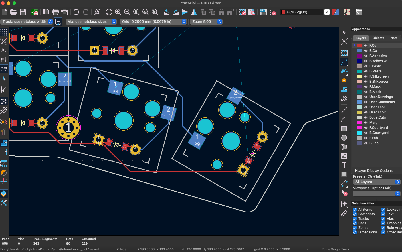
This particular diode footprint has SMD pads on the front and back. To start with, wire the front pads to the through holes. To do this, hover over one of the pads, press the x key to start routing, and then click the lit up pin next to the pad. Repeat this process for the other pin and pad.

Flip to the back layer with v and wire up the rear pads. Again, x to start routing, click to stop. Yes, this is going to get a little tedious doing it on the front and back for 58 keys.
Next, wire up the through hole pin on the right to the pad on the right. When you're actively dragging the line, the two should be lit up so you know where to draw.
KiCAD has a bit habit of sometimes jumping to a gap you didn't quite expect. If this happens I haven't found a good fix other than wiggling the mouse a bit or tapping Esc to cancel routing and remove the line. Sometimes you just need to try drawing the route a few times. Starting from the opposite end can also sometimes help.
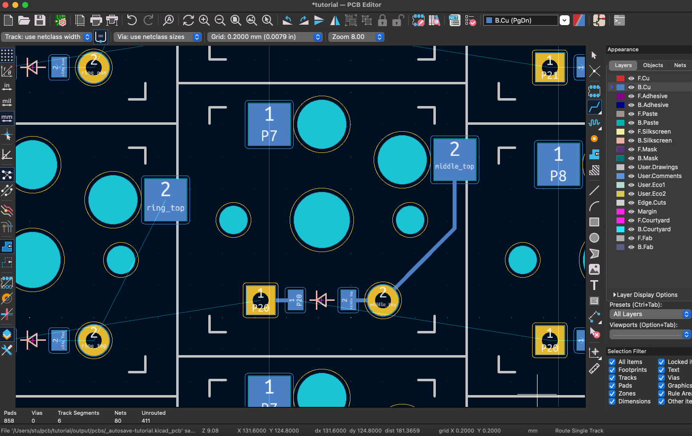
Repeat this process for 9 different switches. (Naturally you don't have to stick to this design exactly, but having a repeatable per-switch footprint does make your board look nice.) Now that we have several adjacent keys, we need to figure out how to wire them together.
Pressing x over a pin will show us everything it's supposed to connect to. If we do it on the right side of a side, we can see it's connected to the right side of the SMD diode pad, and the right side of our hotswap pad.
If we do this on the left side of the diode, we can see the entire row light up. Now we're in business! Use your new routing skills to wire together three keys in a row.
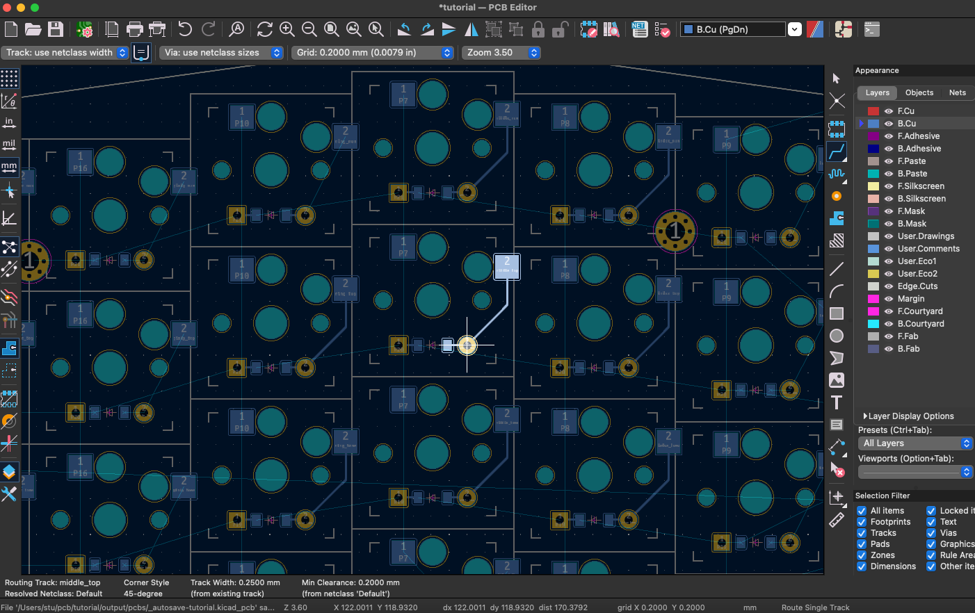
While routing, you can click your mouse to lay down the trace you've routed so far. If you like the first part of a path, clicking lays that part down so you can start using it as the anchor for the rest of your routing. Now that we have a row set, let's take a look at a column.
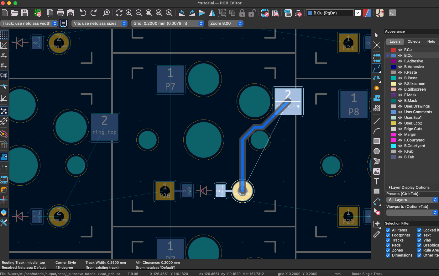
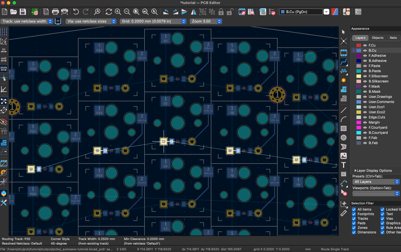
Well shoot. The columns are all connected together by the SMD pads on the left side of our hotswap socket. All of these pads are blue, which means they can't cross over the rows we just routed. We could start using vias to hop the rows here, but let's try to be a bit more smart about it. The columns are forced to use the blue SMD pads as their start and end points, but rows start and stop at through hole pins. We should go back and re-do those rows as front traces. Thankfully KiCAD supports Cmd/Ctrl-z.
There we go! We now have a nice repeatable pattern we can use to wire up every key. The left side of the hotswap sockets are all connected together in a single column. The right side of the hotswap socket connects to the right side of our diodes. The left side of our diodes are all connected together in a single row. When a user presses on a key, the left and right pads of the hotswap socket will be connected together. They'll form a single circuit, passing through the diode on the way back to the microcontroller.
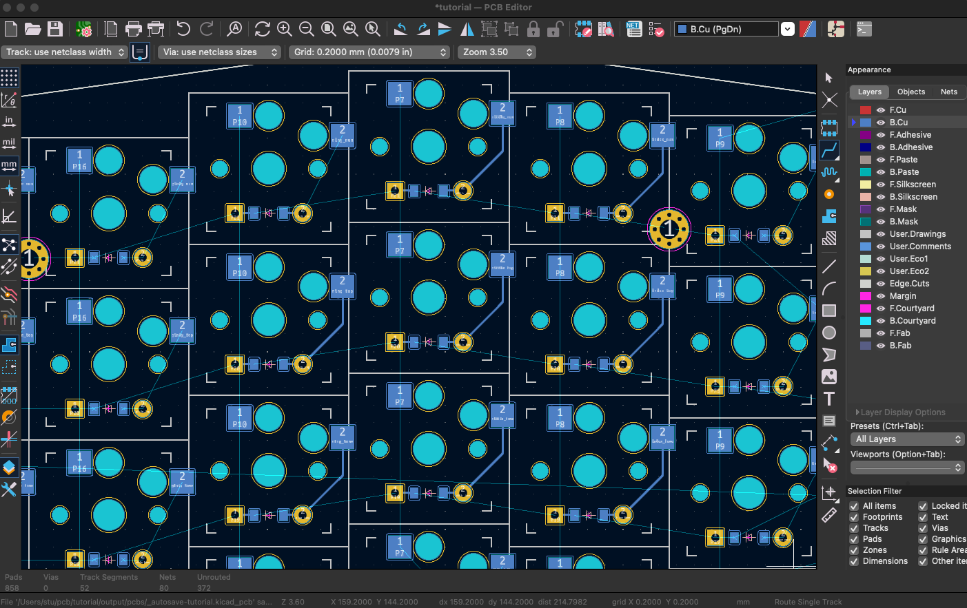
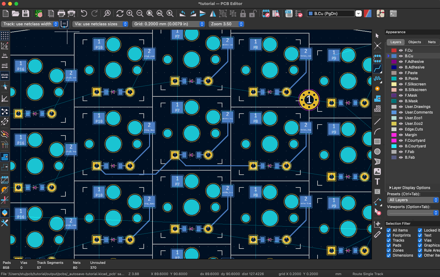
Now that we've got the base pattern down, it's time to apply it to the rest of this side of the keyboard.
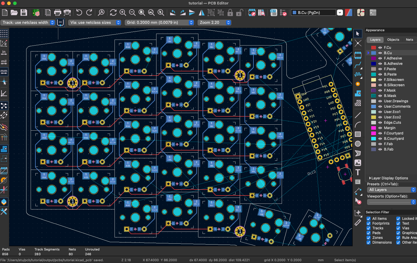
Looking good so far! The top four rows have all been traced using the steps we covered before. Hopefully you've figured out KiCAD's slightly wonky mouse wheel scrolling by now. (It zooms in on wherever your mouse is hovering when you scroll.) The only big routing piece to call out here is the modifier keys on the bottom. Their columns are all shifted over by one, so we have to be a bit careful how we wire those up.
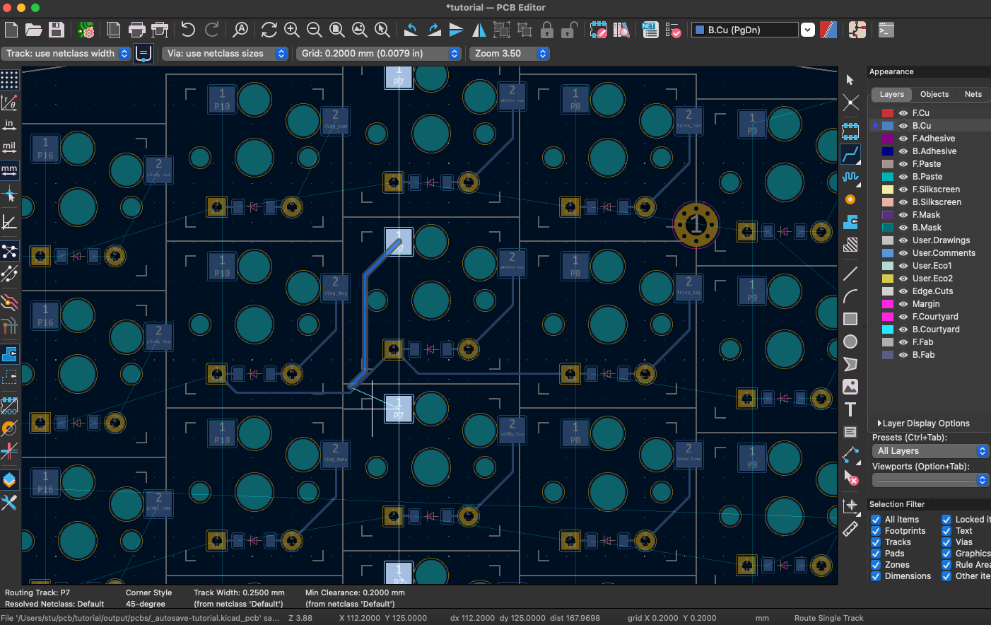
I've also gone ahead and routed the two thumb keys. This is a good example of what happens when you don't rotate the PCB before routing.
Those are some gnarly traces. Let's go back to the Preferences and set the "Step for rotate commands:" to 15 degrees.
There we go. That's marginally cleaner. Now we can set the rotate step back to 20 degrees.
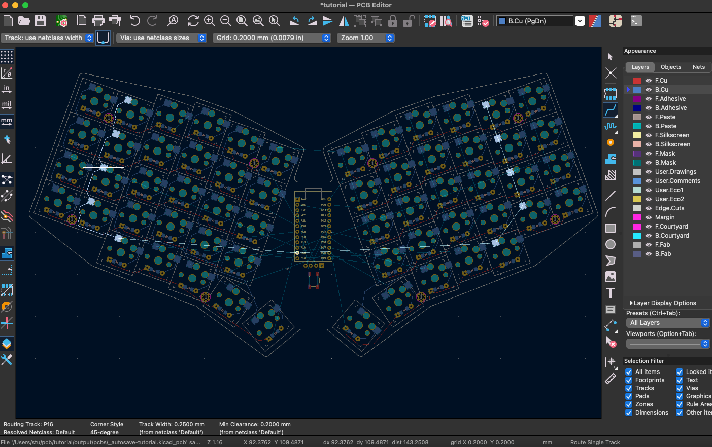
With that, we're done with the left side of the keyboard! Press Cmd/Ctrl+a to select all of the parts, and then Shift+r twice to rotate things over to the right side of the board.
Time to do all those routing steps all over again. You've got this, right?
Yeah, you've got this. Alright, we have the two halves of our keyboard matrix wired together. What next?
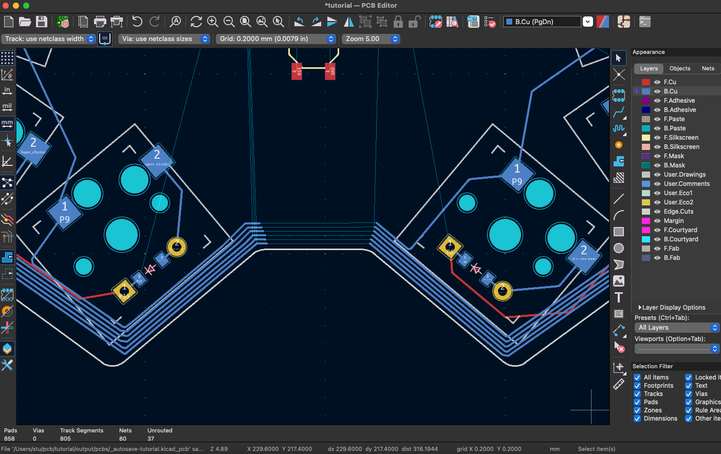
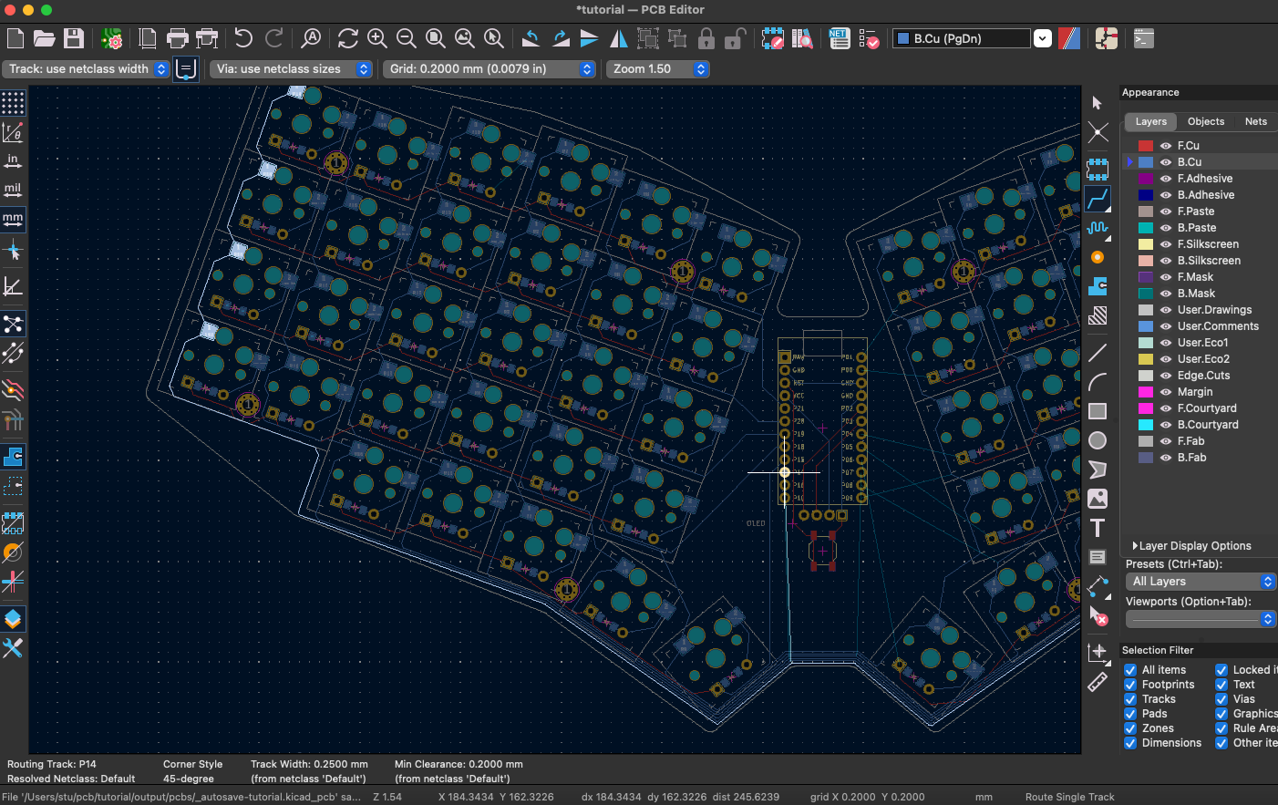
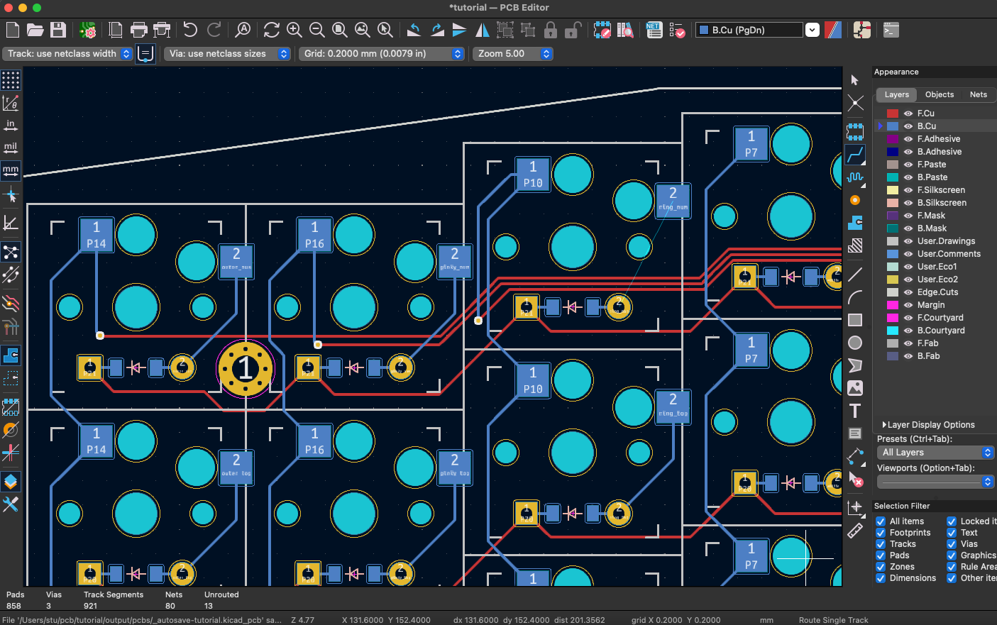
In Part 3 of this guide, we touched briefly on keyboard matrix theory. This keyboard is using a "western duplex" matrix. The columns are technically stretched out to cover both the left and right side. If we start routing from one of our left hotswap pads, we can see both parts of the keyboard light up.
Things are going to get a little tight, but we should be able to run a set of traces along the bottom of our keyboard. Start from the outside and work your way in.
You don't need to finish the routes all in one go. In this screenshot, I've routed a trace for the outer, pinky, and ring columns along the bottom of the board. I like working on one side of the board, leaving a half-finished trace, and then coming back to it later after you've routed the board. Unfinished traces will work just like pins and pads on your board, and will have their associated nets pointing off of them.
When routing traces closely together, KiCAD will show a small transparent area next to your route. This is a minimum buffer area between the traces to keep them from interacting with one another. The KiCAD's default distance should be fine for our keyboard.
There's all six! It's not the prettiest group of lines, but it'll do the job.
You may need to get creative with your rotation angles when routing around some of these corners. Changing your Grid settings may also help.
If you routed everything properly, the nets should match up when these two groups of lines come together.
Holy cow that actually worked. Connecting all the lines took a bit of fiddling, but they came together in the end.
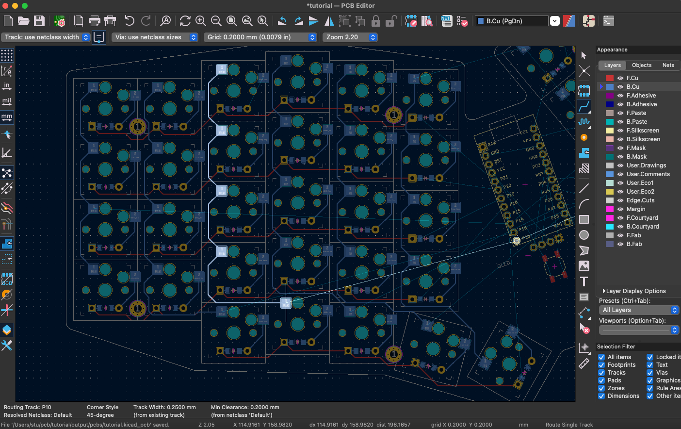
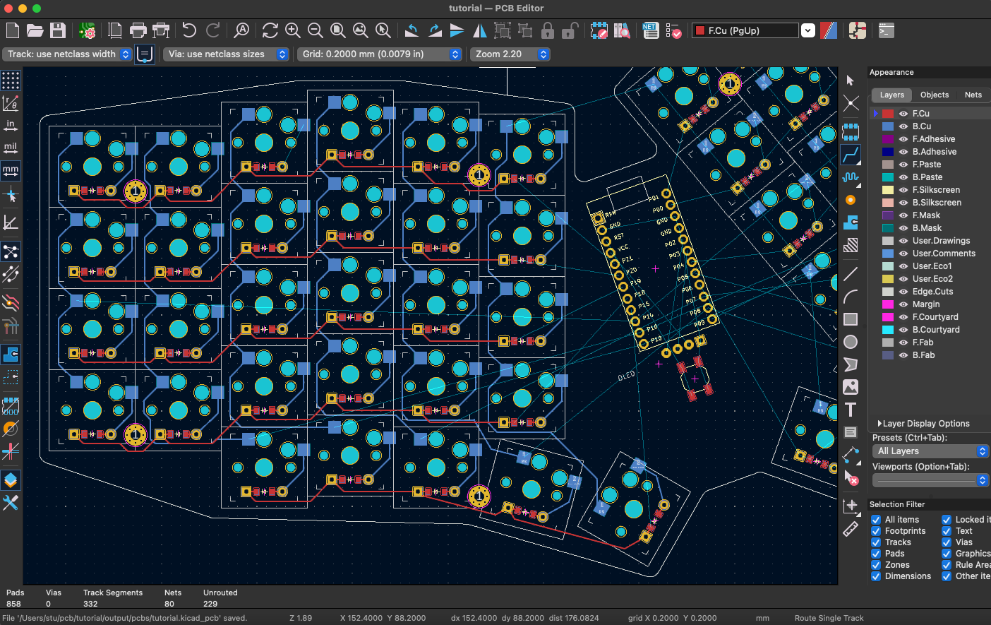
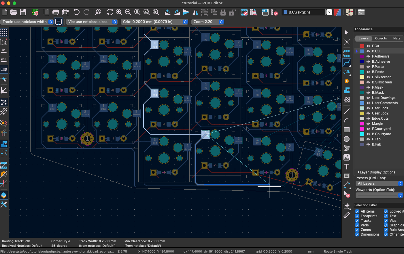
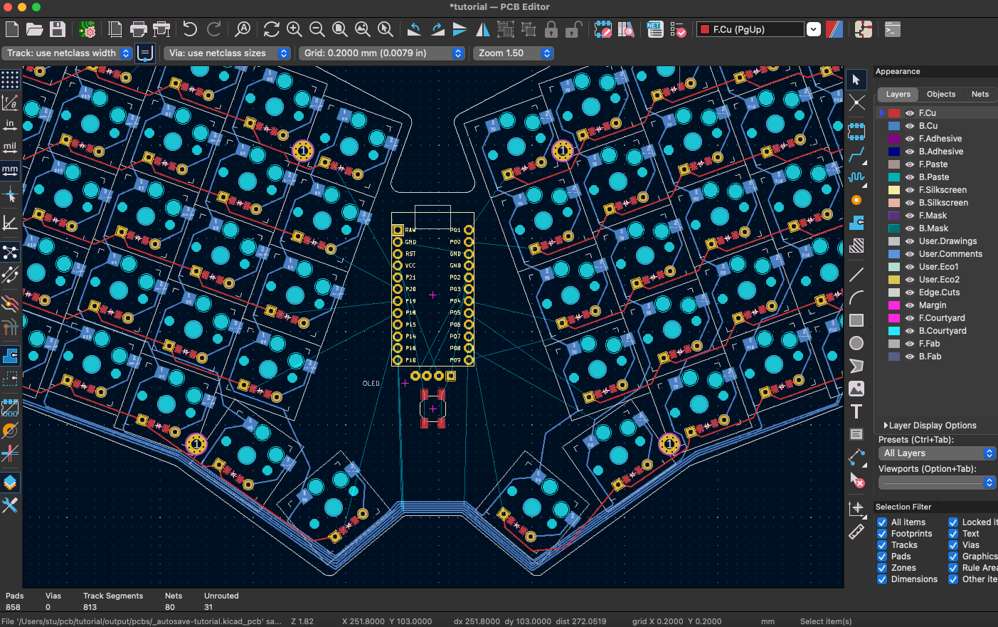
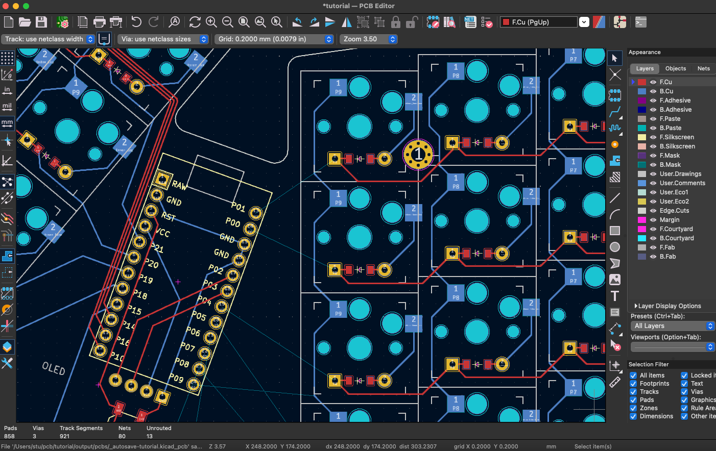
Okay. So. Microcontroller time. I like routing the OLED screen and Reset button to start with so that the nets are a little more readable.
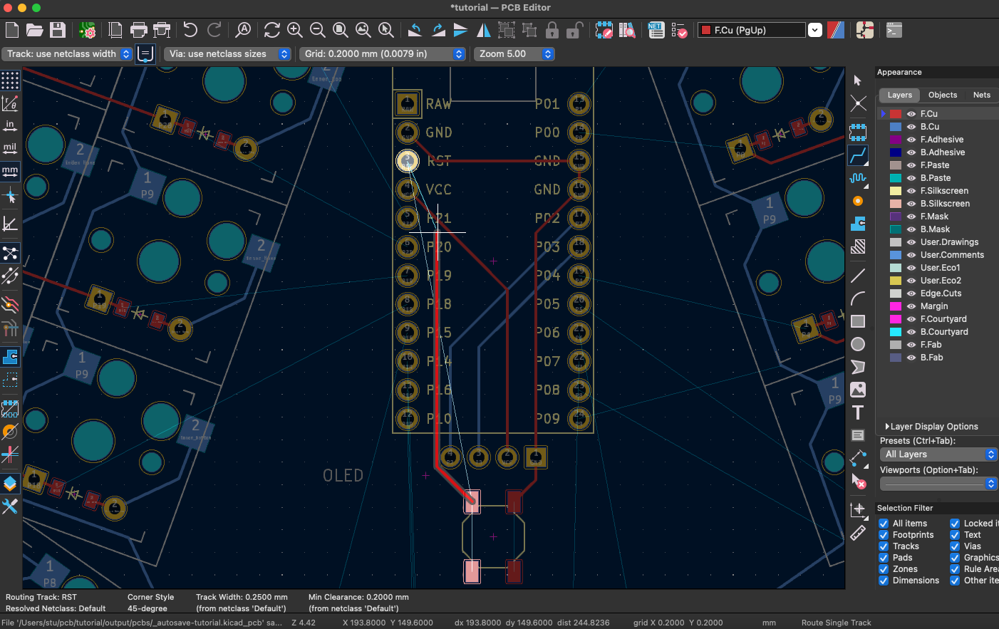
You generally want to keep all of the microcontroller accessory routes inside of the microcontroller's footprint. We'll need the space to the left and right to route the rows and columns in a minute and- Ugh. Hold on.
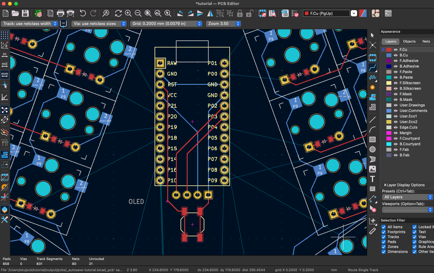
There we go. Routing these things takes a lot of trial and error. Give yourself time to figure out the best layouts for things, and don't be afraid to back up and do sections over if you need to.
As a random aside, you'll notice all of the GND ground pins routed together here. They're technically connected together internally on the microcontroller, so these traces are strictly necessary. However, I've totally botched a header pin on a microcontroller in the past, so it's always nice to not have to rely on a single pinout if you don't need to.
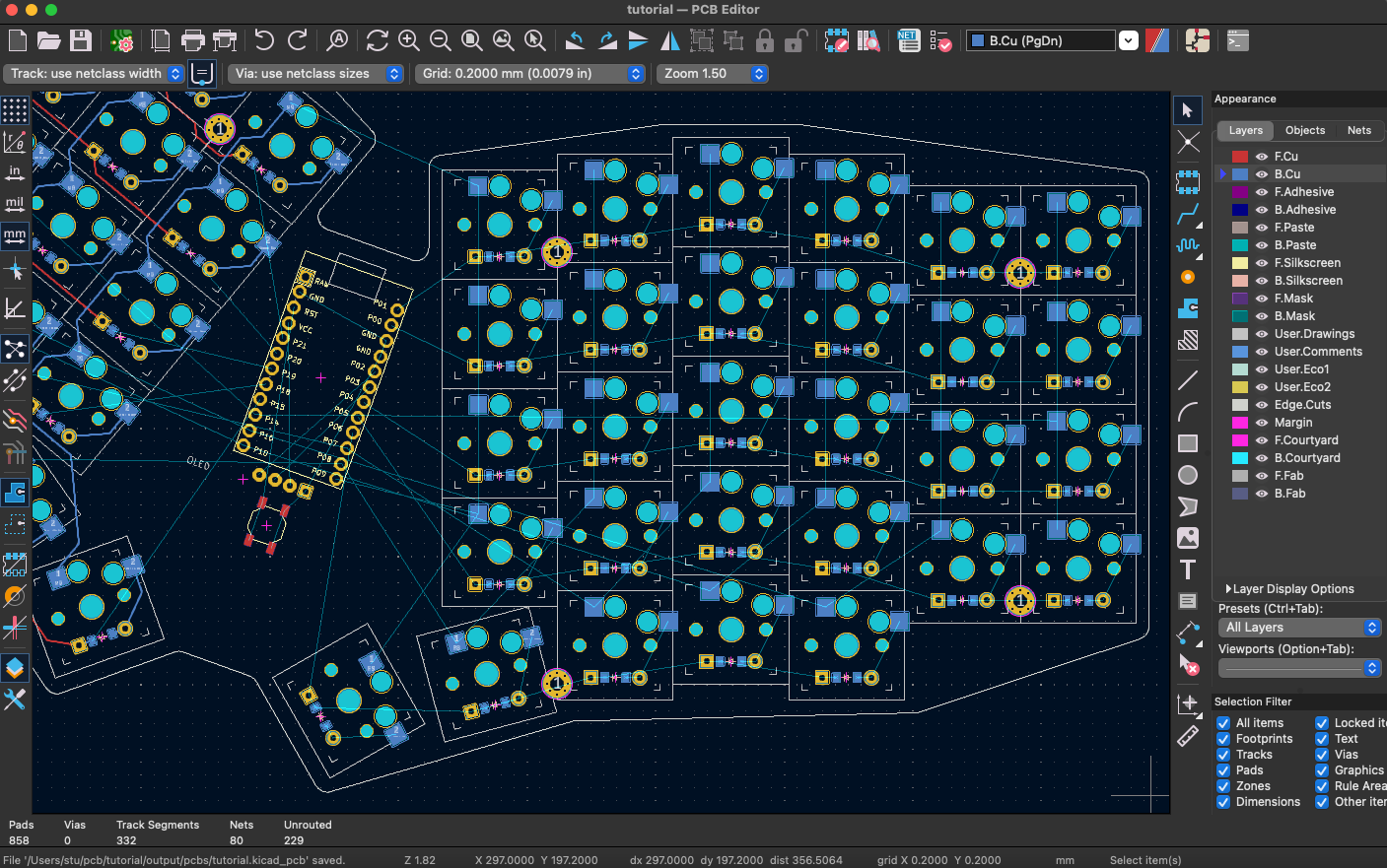
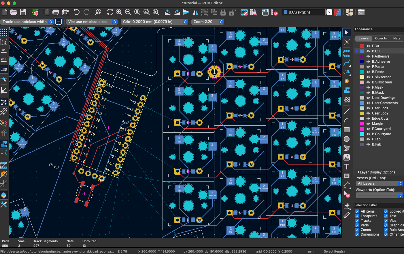
Our traces are a bit more readable now. The column traces are mostly pointing straight down, but we can see the row traces reaching out. Let's connect those now.
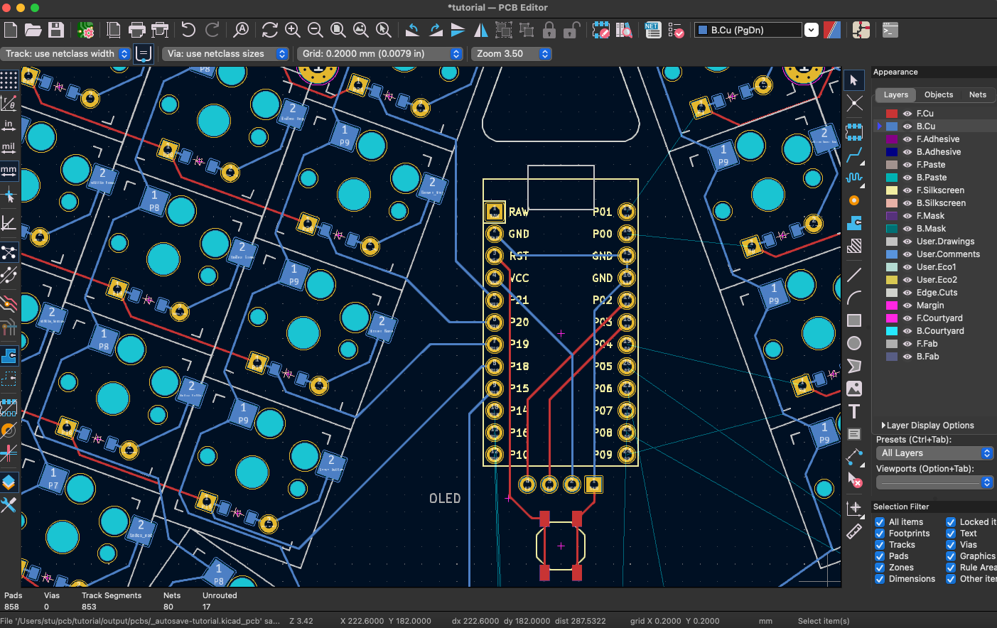
These traces are admittedly a little messy. They get the job done though. Feel free to rotate things back and forth as you route if you haven't been already.
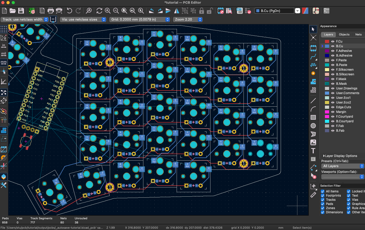
When routing a PCB, it's important to remember that the F.Cu traces are the ones you're more likely to see. We can be a bit more clean for the next step.
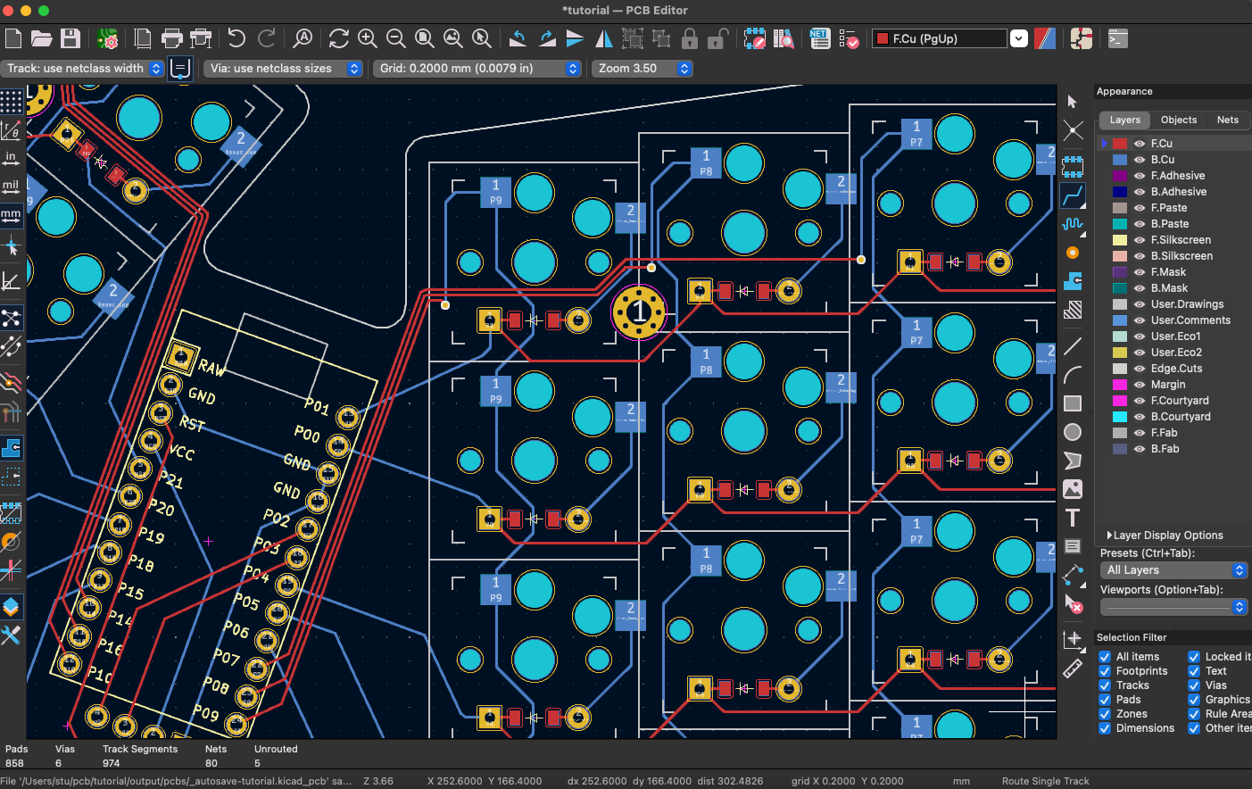
The majority of our board is routed using back traces. The only piece of our matrix using front traces are the left-to-right row traces. This makes things a bit easier to get across the length of the board. Let's start our column routes off with some red F.Cu traces.
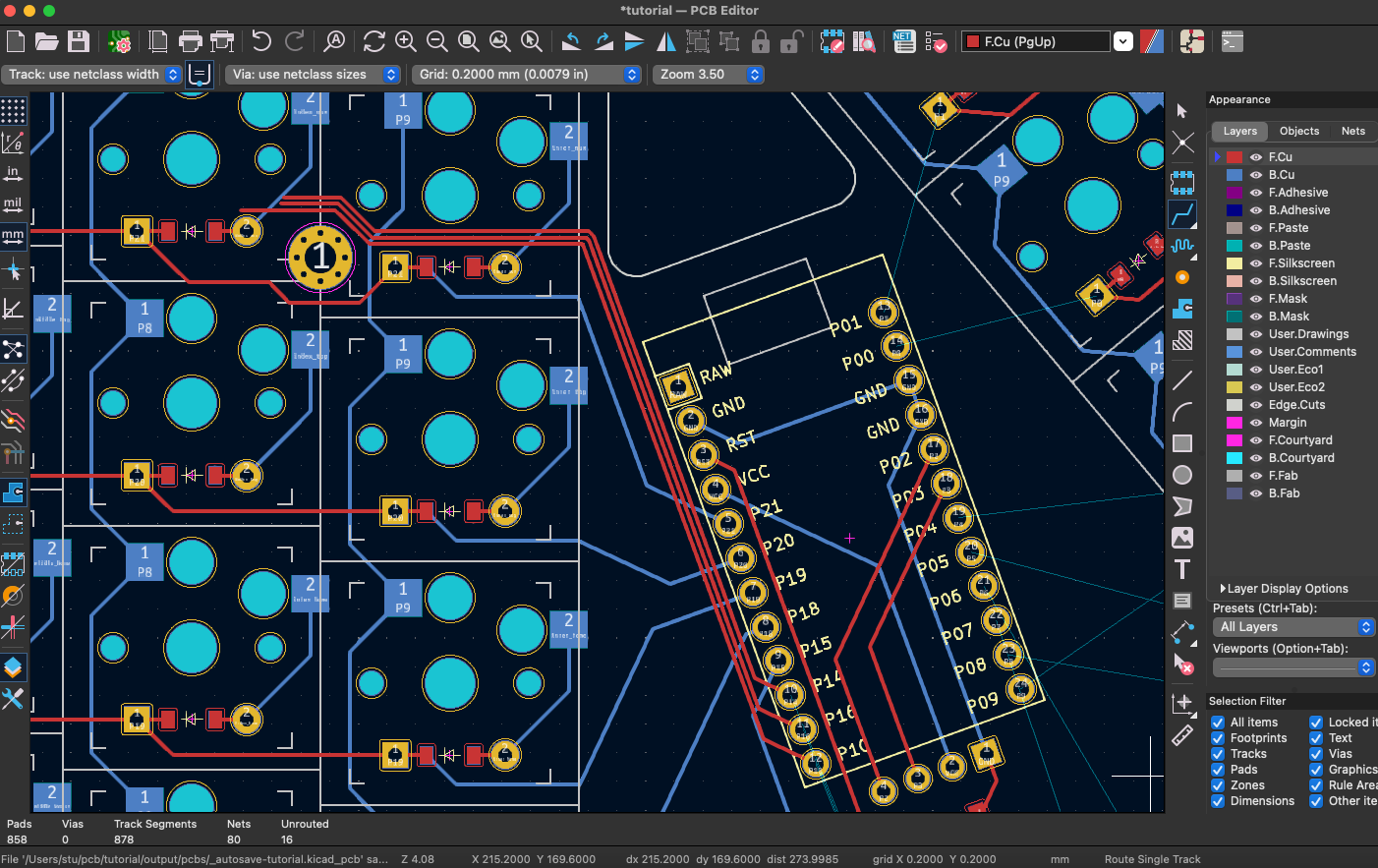
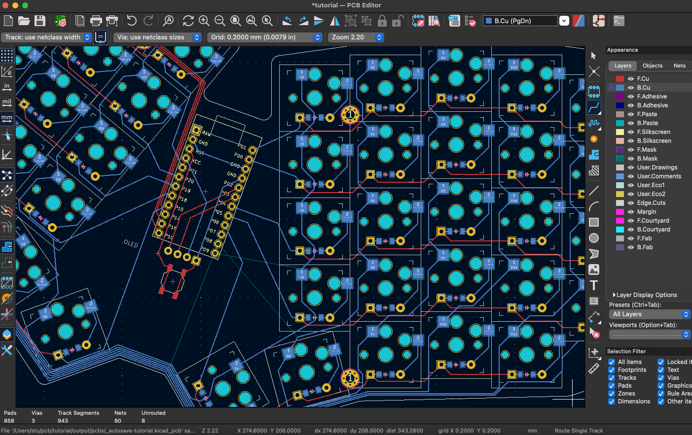
Now there's a nice trace. Nice symmetrical straight lines framing our Arduino. That should look good on the front of the board. Once we start routing under the keys, we don't have to worry as much about all our traces being perfectly aligned.
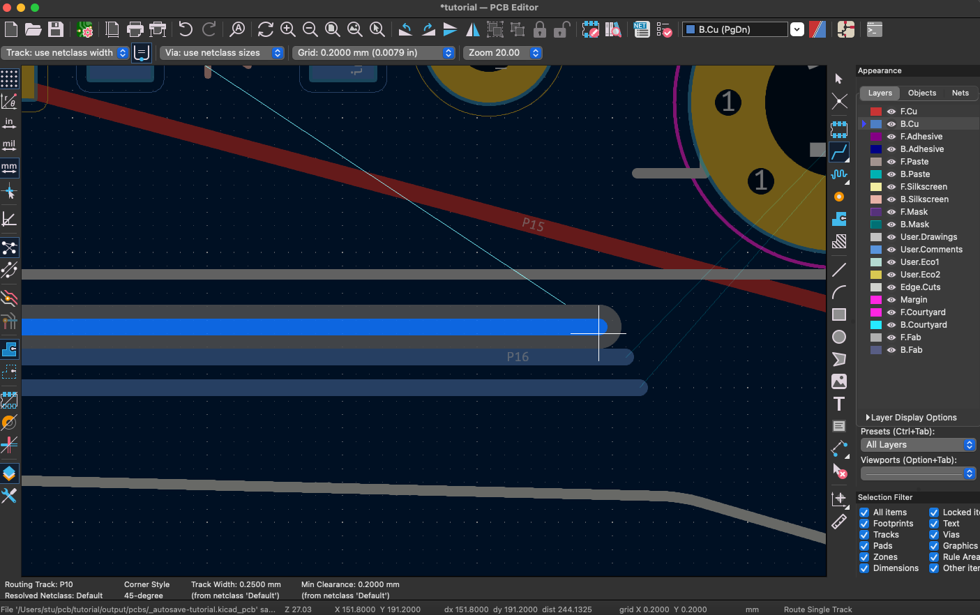
Finishing off these routes marks the first appearance of vias in our keyboard. The F.Cu traces made it easy to travel this far across our keyboard, but in the end we still need to connect to a pad on the back of the board.
Okay, time for my coffee break. Do that again but on the other side-
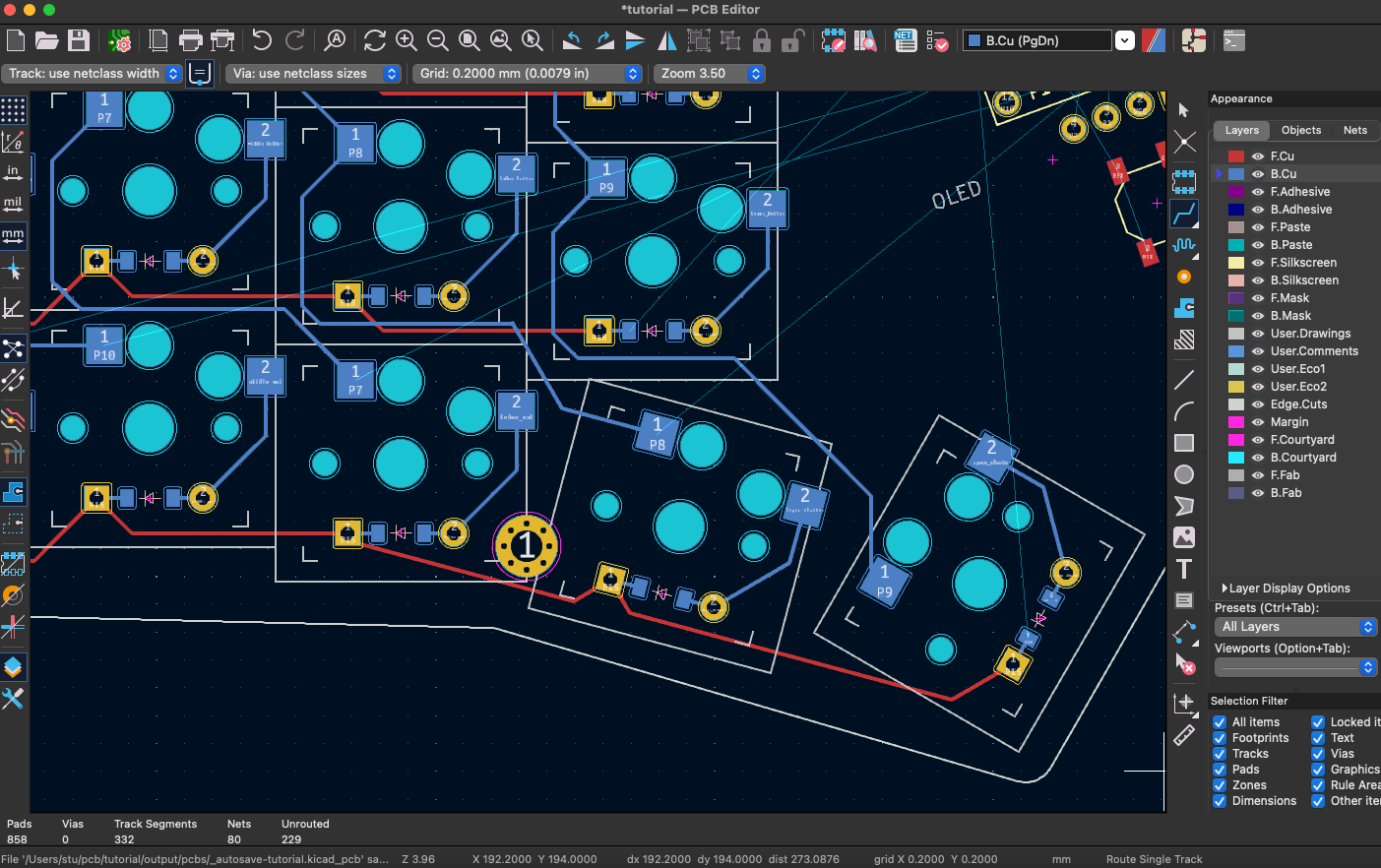
Wait, what do you mean there's a trace in the way? Right, our board's symmetrical, but these key switch footprints are not. The column traces on the left side of the switch are in the way if we want to use the same row routes as before. Is there any way we could get them out of our way? Hmm...
Routing through diode footprints is a little cheeky, but it'll work in a pinch. Just be careful when soldering that column of diodes and you should be fine. Probably. The good news is we can route our rows now.
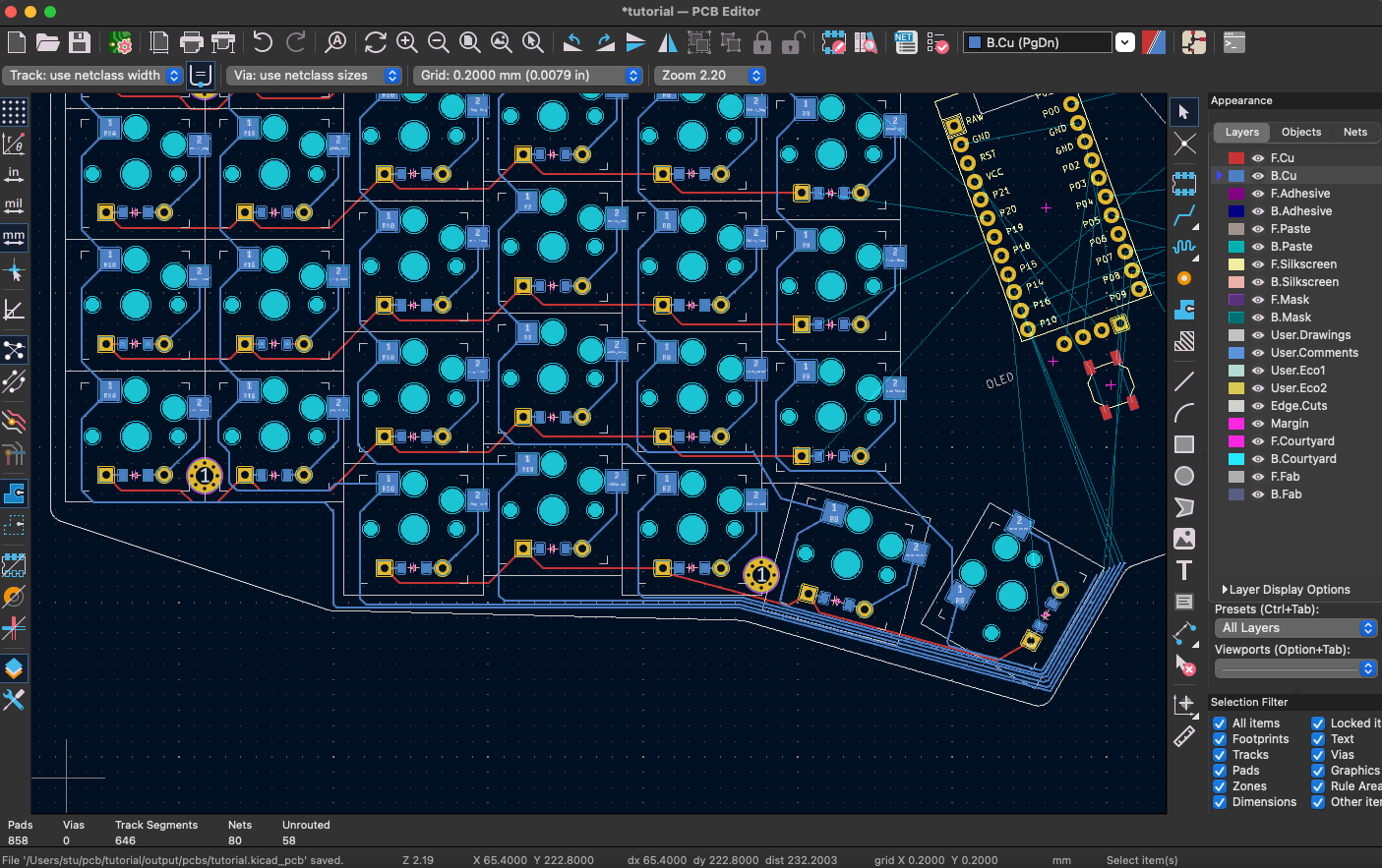
There we go. Now we just have three more columns to route. Thankfully these don't have to go as far.
Three more traces, three more vias, and we're done.
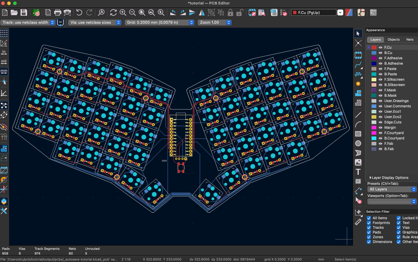
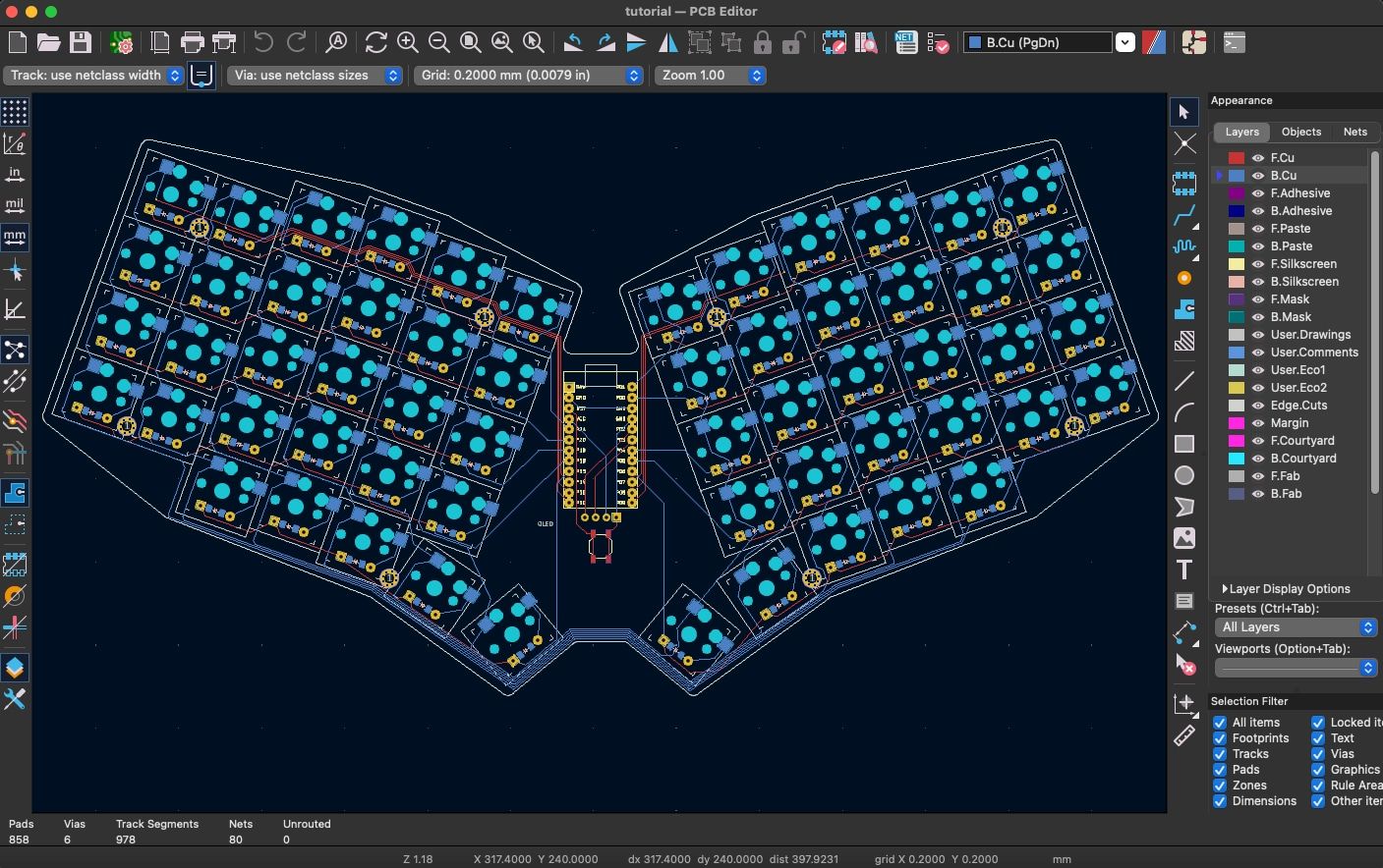
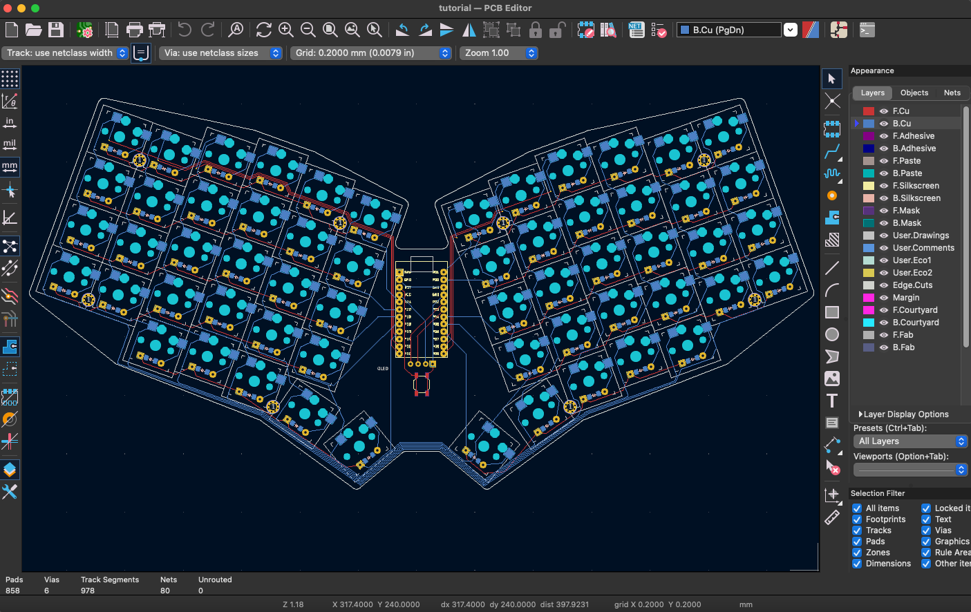
Wait a second. We're done! Look at that! A shiny new keyboard, all routed and ready to send off to the fabricator. Go us! We're finished with KiCAD now, right? Well, not quite.
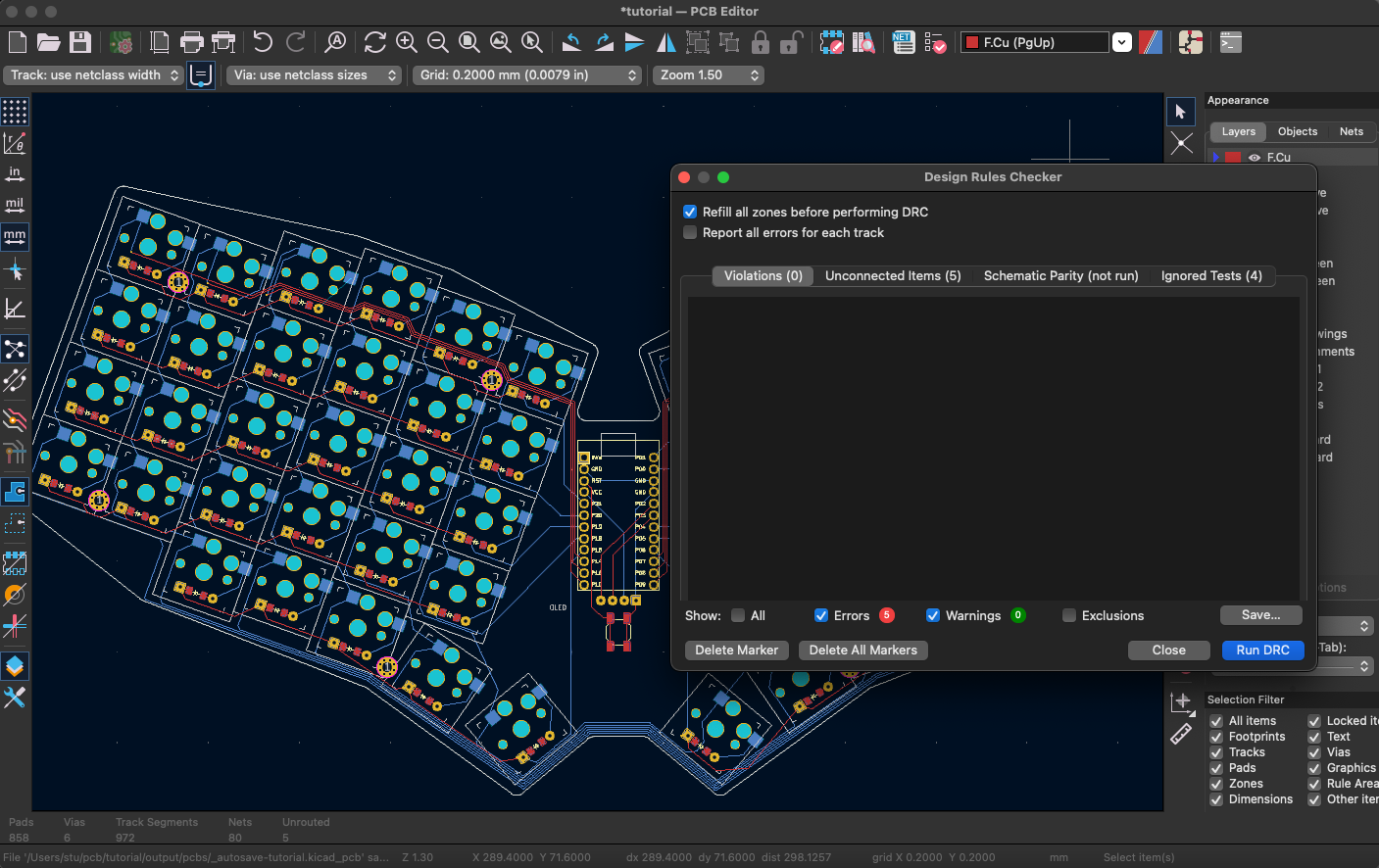
Design Rule Checker (DRC)
Chances are you made a mistake somewhere in your board. (It's okay, this is a judgement free zone.) Rather than having to meticulously scrub through every trace however, KiCAD has what are known as "Design Rules". They're a set of configurations that stop us from making easy-to-spot mistakes like laying two footprints right on top of one another, or leaving a pad un-routed.
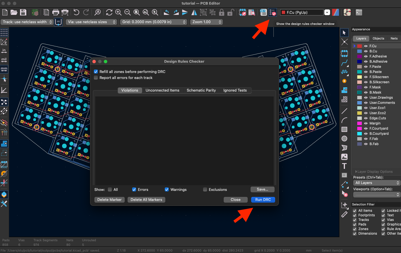
To access the DRC tool, click it's icon on the top navbar. Then click Run DRC in the modal that appears.
Oh jeez. That's a lot of errors. I was expecting one or two. Not over a hundred. Did I mention I upgraded to KiCAD 7 at the start of this guide? Hopefully this is just a quirk of the new version or some side effect from upgrading. Still, I'll keep the resolution of these issues in the guide if only for demonstration purposes.
Let's start with the easy warnings. Clicking on an error moves your window to that portion of the PCB. Zoom in on your board, then click the error in the DRC window to get a better look.
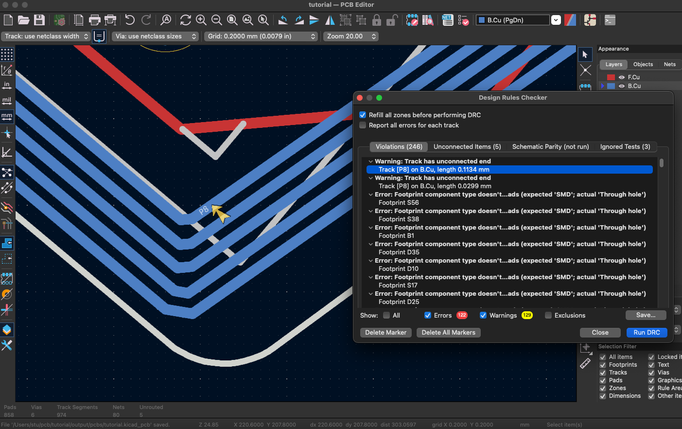
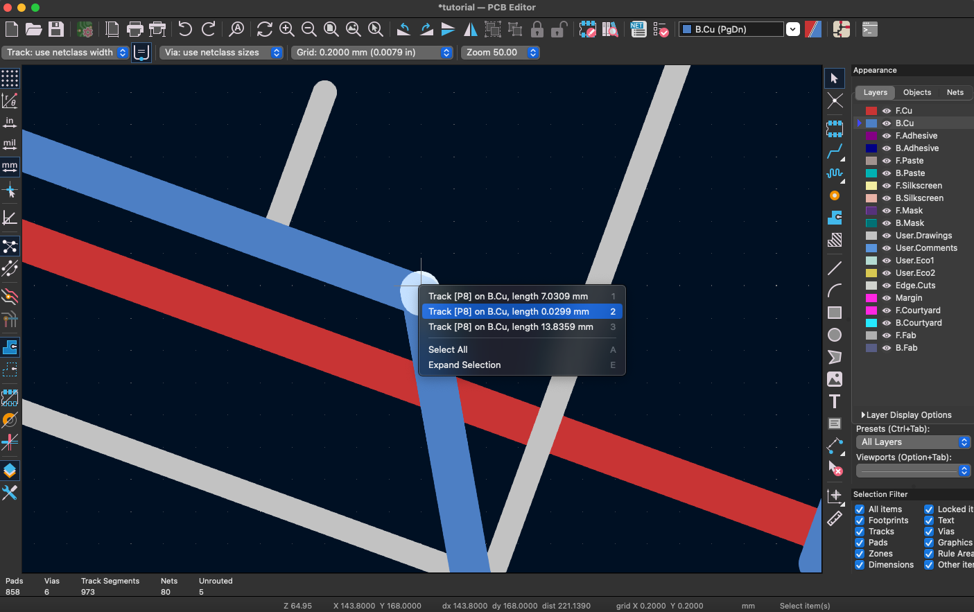
KiCAD's router can sometimes leave small orphan fragments on your board. If you click where the arrow is pointing, you'll get a dropdown asking you which trace you're trying to select.
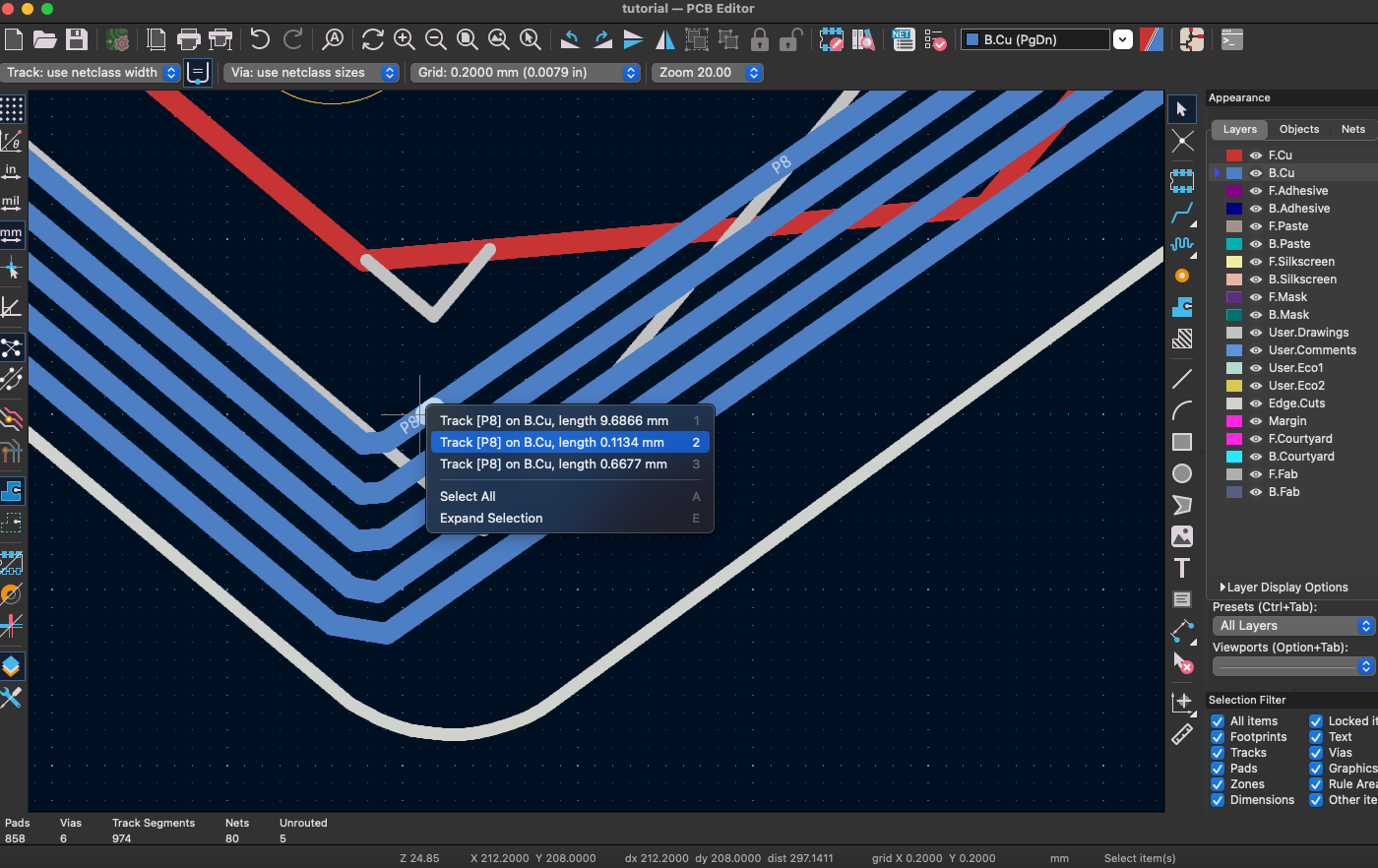
Pick the small stray segment and delete it. You can delete traces with backspace on your keyboard.
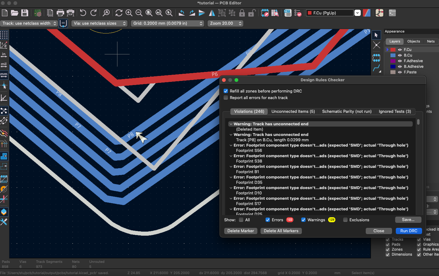
If you fixed the issue correctly, you'll see [Deleted Item] in place of the track definition. The arrow will linger around until you re-run DRC however. (Or until you click the "Delete All Markers" options.
The other error had a similar chunk of trace left at a corner.
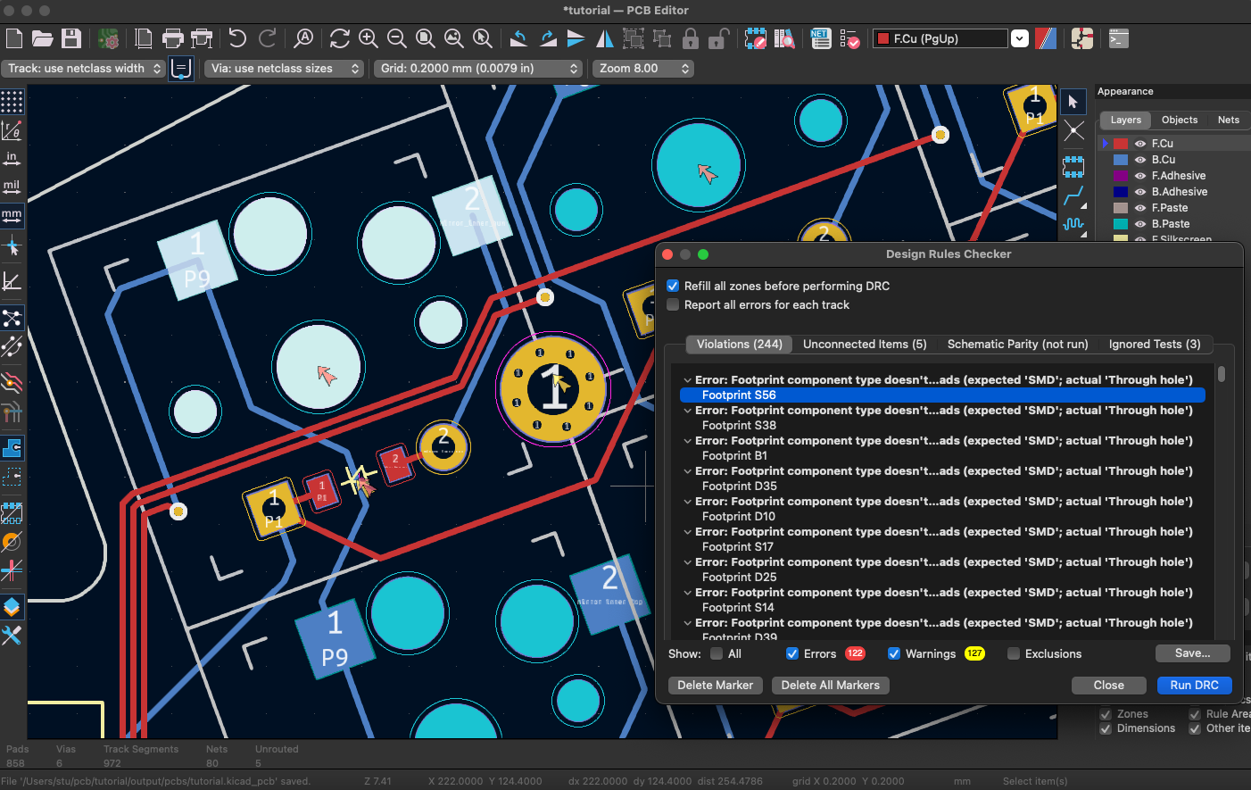
I honestly have no idea what's going on with the next error. Apparently the footprint has an incorrect attribute? Let's double click on the switch and figure out what's going on. If you double click on a component of the footprint (a pad, drill hole, etc.), you'll get the properties of that component. We want the properties of the entire footprint, so double click on some of the whitespace in between. You can also right click and select Properties... if you're having trouble finding some clickable whitespace.
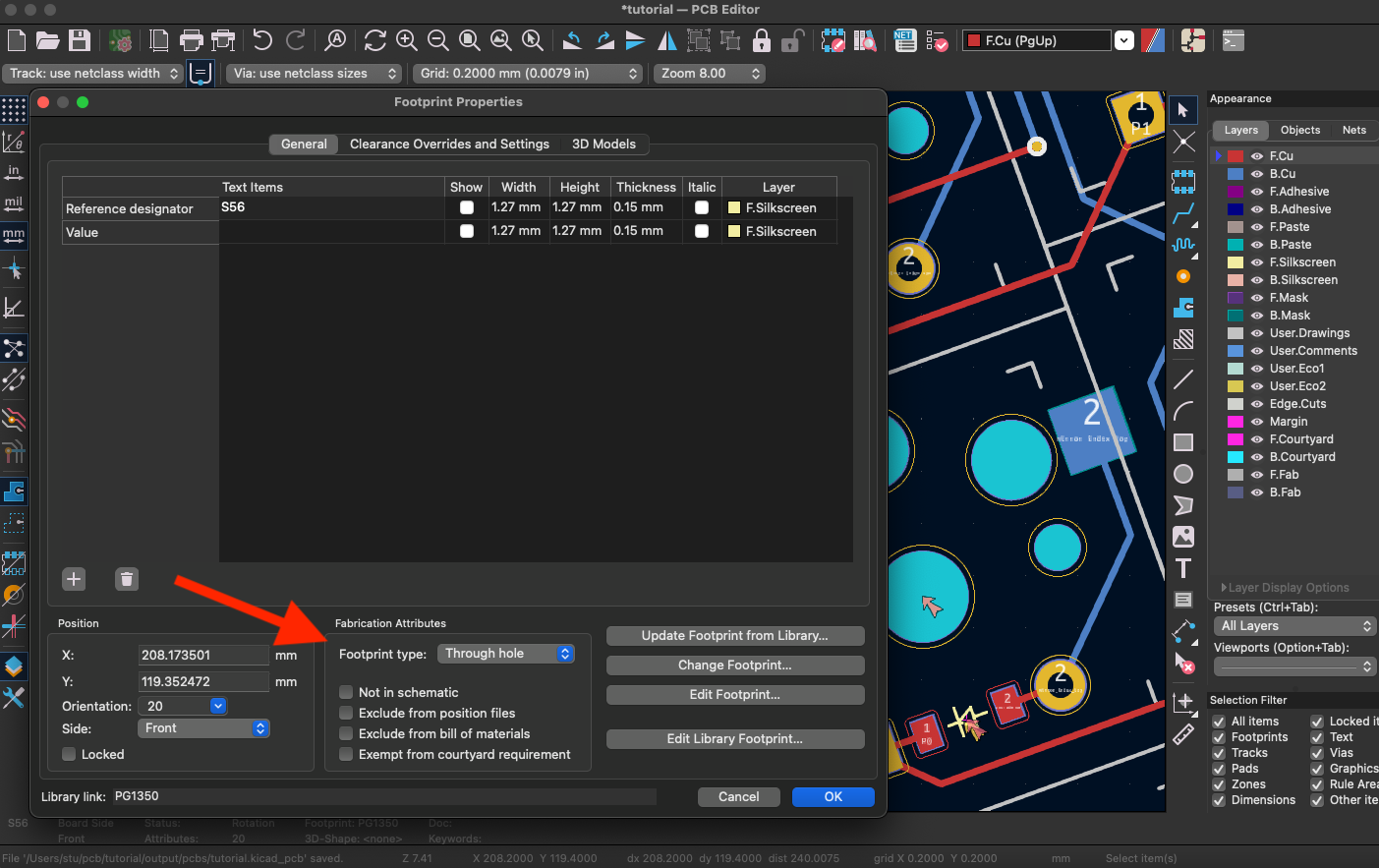
This appears to be our culprit. Change "Footprint type:" to SMD. While we're here, it's worth remembering this "Position" section of the Properties screen. It can help you align footprints or tracks when laying out a PCB. You can also toggle the checkboxes in the "Show" column to enable or disable some silkscreen markings on your board.
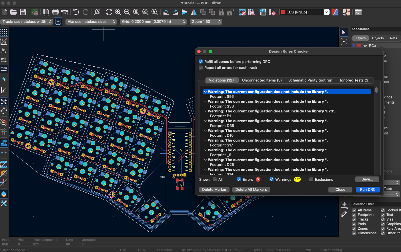
Changing the "Footprint type:" on all of our Choc footprints and the diode footprints appears to have resolved this error. The next group of warnings has me stumped though. Hopefully this is just a side effect of updating KiCAD halfway through a tutorial? Or maybe it's something about Ergogen's footprints that KiCAD 7 just doesn't like. Either way, these are just warnings. Thankfully we can clear these out rather quickly.
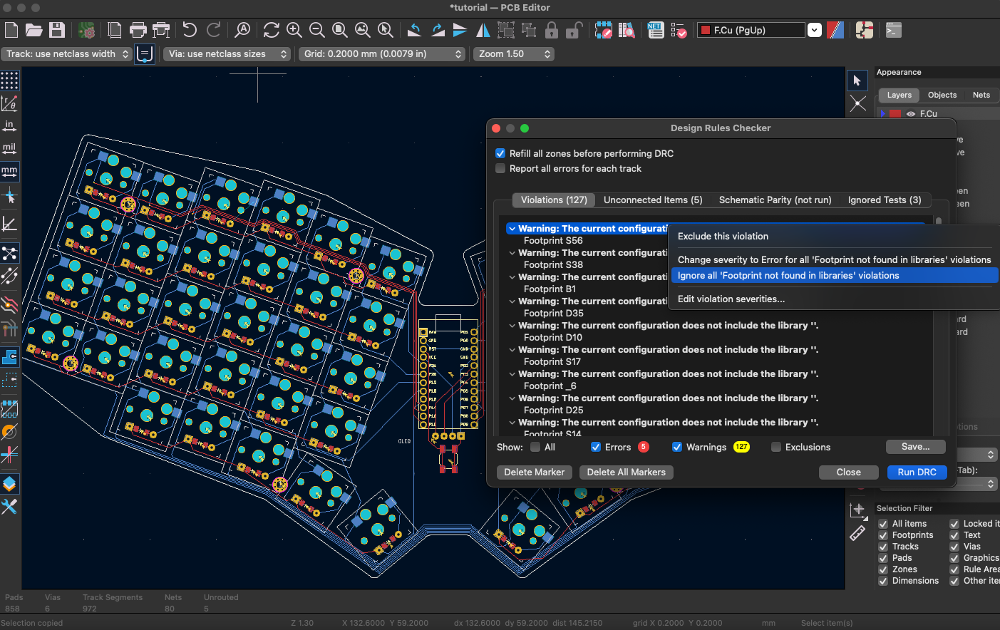
Right click on one of the warnings and then chose the Ignore all 'Footprint not found in libraries' violations option.
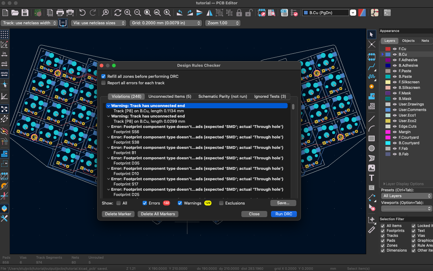
That cleared out all of our errors and warnings. There's still a few issues under the "Unconnected Items" tab however.
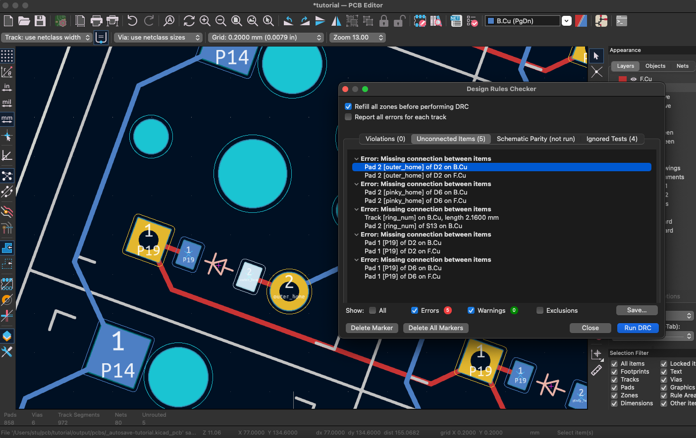
Alright, here's the feature of DRC I actually wanted to show. The Unconnected Items tab is great for finding diodes you forgot to wire together on one side of the board.
The stock Ergogen footprint has two through holes, and then two sets of surface mount SMD pads. Both the red pads on the front and the blue pads on the back need to be connected to the through holes next to them. If you run DRC and get a number of errors that is close to 2x the number of keys on your keyboard, you've probably forgotten to connect the SMD pads on the back side of your keyboard to the through holes.
Looks like I missed a hotswap trace too. You can actually see this mistake in the 6th from the last screenshot in the routing section of this guide. Let's pretend I left it here as a learning example. Running DRC at the end of your routing process is vital for picking up small but critical mistakes like this.
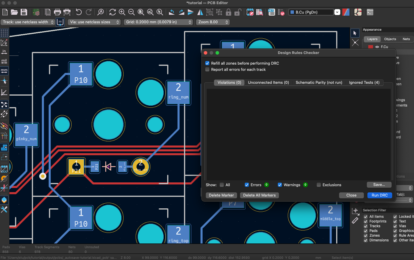
Once you've finished correcting all the issues, run DRC one last time to verify that your PCB doesn't have any errors. Looks like we're good to go.
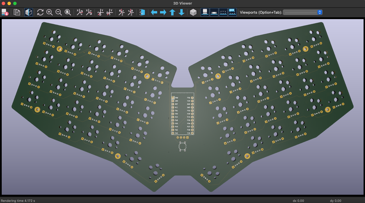
Surely we're done with our board now, right? Well... Let's take one last look at things. It seems fine, but humor me and select View -> 3D Viewer from the file menu.
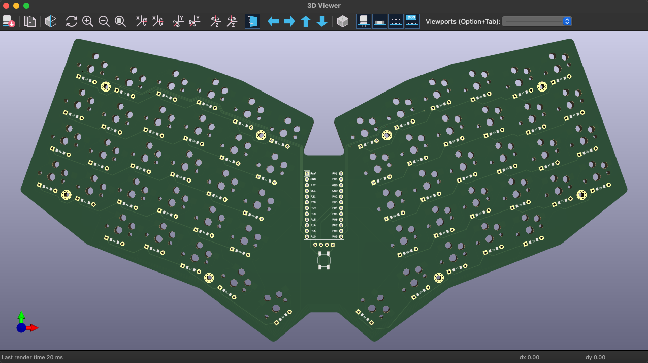
Tada! Here's a render of our board in all its 3D glory. This view can be good for one last double check. You can make sure the layout of your footprints makes sense, and that there's not an unsightly silkscreen you hadn't noticed.
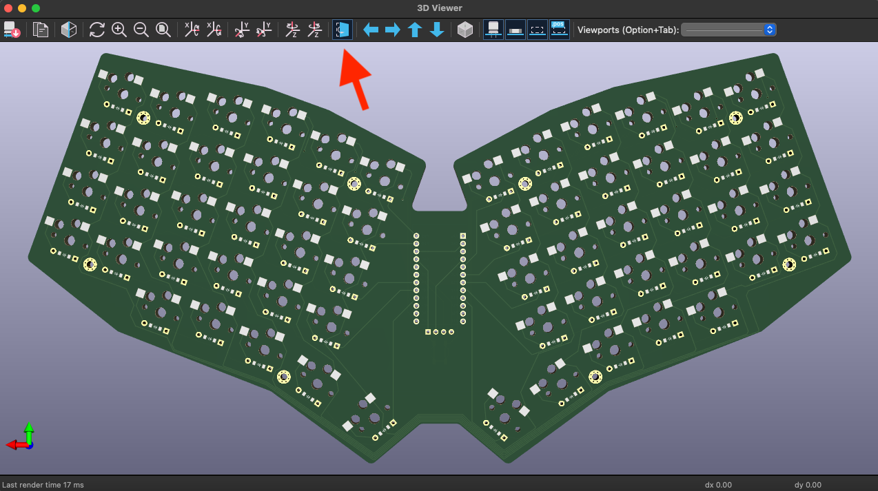
You can spin the board around with your mouse, but there's also a button on the navbar to quickly flip it over.
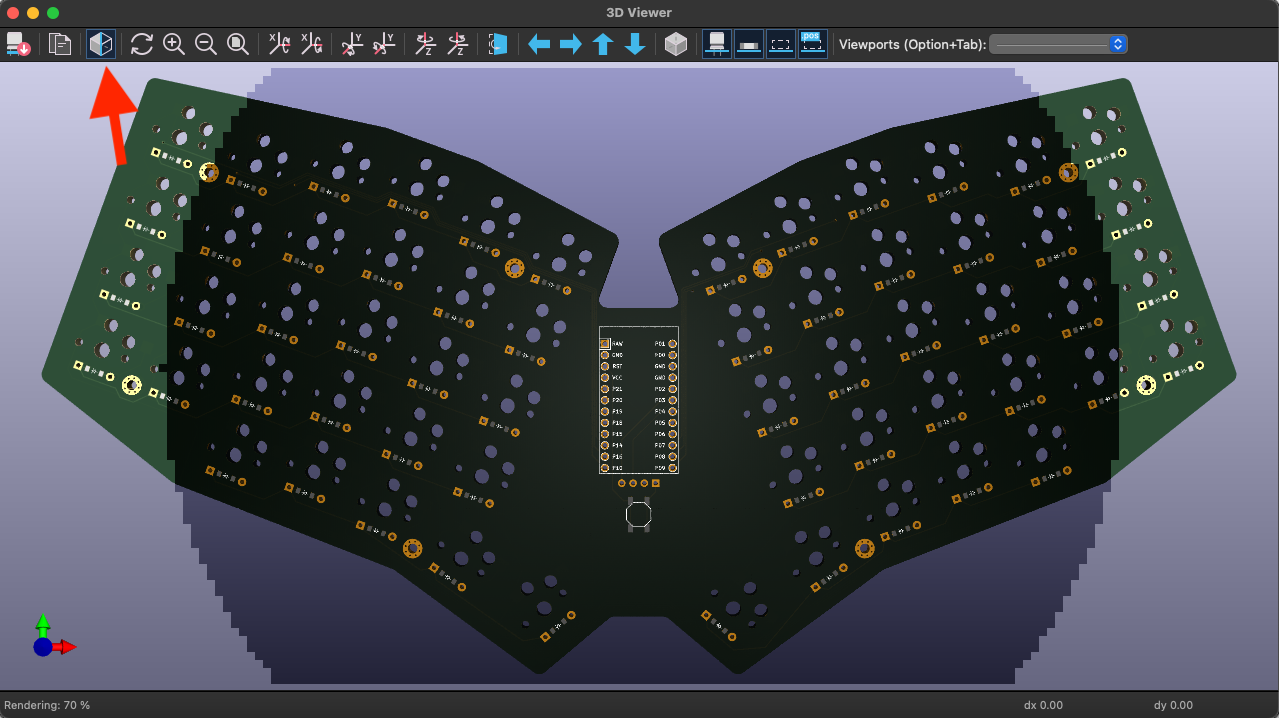
For an added bit of fun, you can click the Raytracing button in the top left corner and watch your system perform a ray-traced render of your board in real time.
Now we're done. That was quite the journey, but we're ready to send our PCB off to be fabricated.
Fabulous Fabs
KiCAD and other software generally use their own propriety file formats. While some PCB manufacturers will allow you to upload a KiCAD or EAGLE file, most prefer it you instead use "Gerber" files. Gerbers have been the common standard for plotting and drilling machines since time immemorial. They're plain text files that are conceptually similar to PDFs. The trick with Gerber files is that's it's Gerbers. Plural. Each layer of your PCB needs its own specific Gerber file. In practice this isn't too tricky. Each layer has a specific file name convention which KiCAD does for us automatically. All you have to do is point KiCAD at a folder and then zip the exports afterwards. Because nothing's every completely straightforward in KiCAD, there's also a separate "Drill" file you need to include in the zip. Thankfully these aren't hard to export either, but it is an extra step.
Once you've triple-checked everything on your PCB, head over to KiCAD's file menu. Hover over "Fabrication Outputs", and then select "Gerbers".
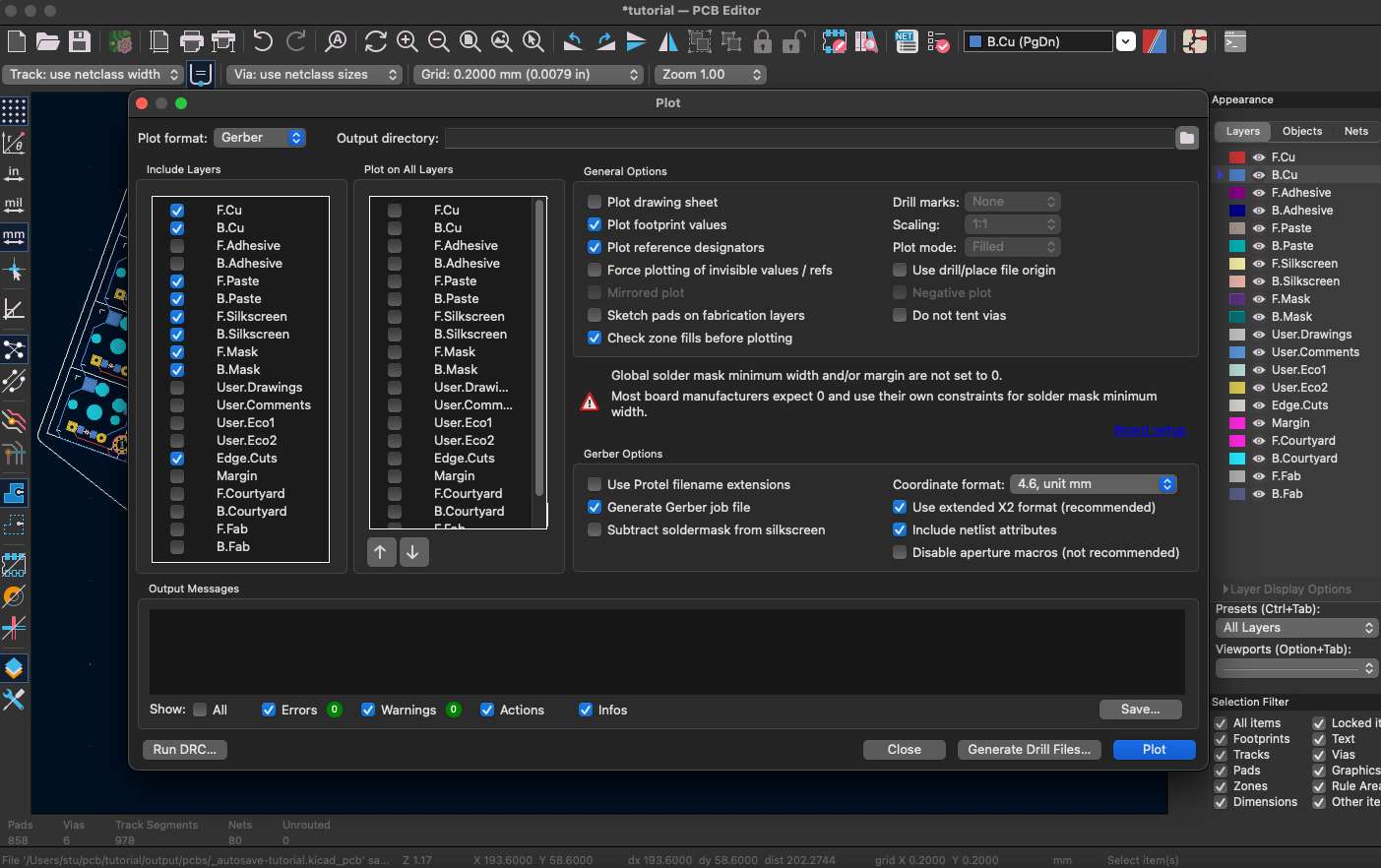
You should be able to stick with the default options here. The Included Layers section will show which layers of your PCB will get exported. F.Cu and B.Cu are your copper layers, F.Paste and B.Paste are used for creating SMD pads, F.Silkscreen and B.Silkscreen contains the text and icons that get printed on your board, F.Mask and B.Mask is the protective coating on non-exposed parts of your board, and Edge.Cuts is where the tool mills away the edge of your board.
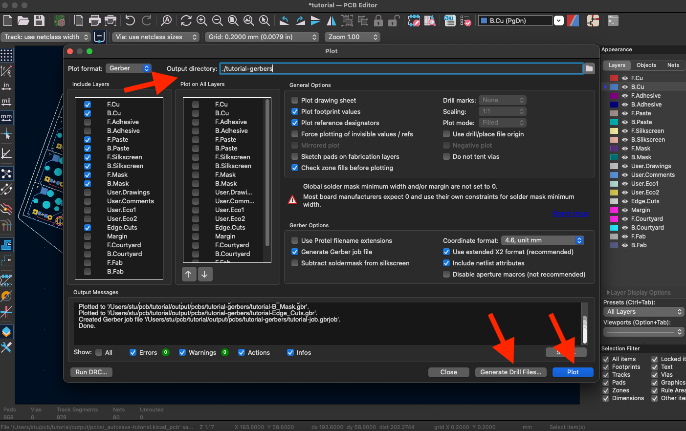
The one change you should make on this screen is to specify an Output directory. By default KiCAD will dump your Gerbers in the same folder as your PCB file. Specifying ./keyboardname-gerbers will create a folder called keyboardname-gerbers in the same location as your PCB file, and then store all of your outputs there. Click "Plot", and KiCAD will create all the specified Gerber files.
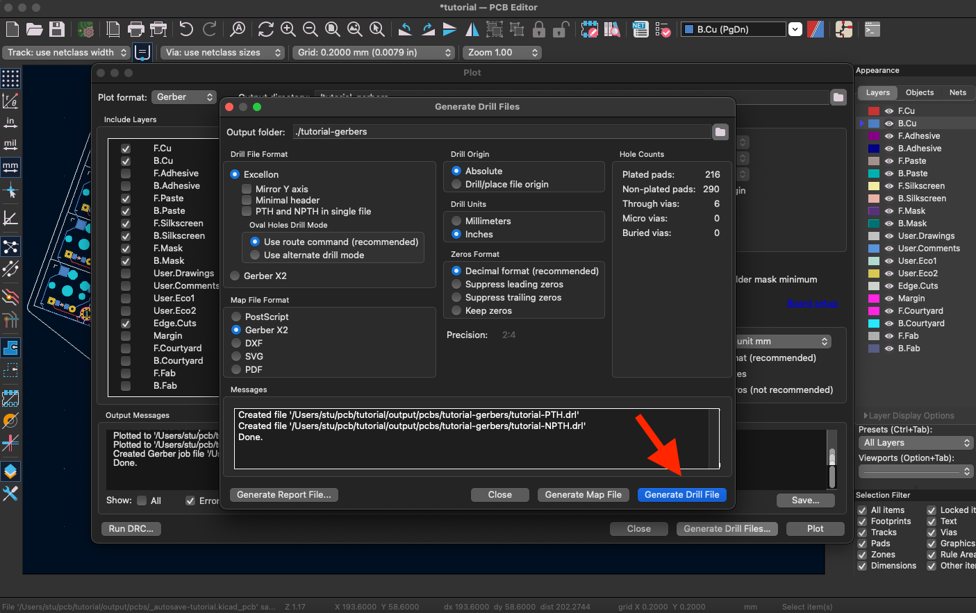
One last step. Next to the "Plot" button, click "Generate Drill Files...". This opens up a "Generate Drill Files" modal. This one last step is needed to tell the machine where to physically drill our through hole pins. You can stick with all the defaults. The drill modal should have inherited your Output directory location from the previous screen. Click "Generate Drill File" and you should be good to go.
Forgetting to create a drill file is a very common step. If you get a message from your PCB fabricator that your upload appears to be missing it's drill file, it's because you forgot to do this last step. Don't worry, it happens to the best of us.
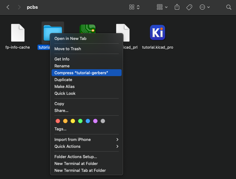
Finally, create a .zip file from your keyboard-gerbers folder. Your operating system's basic compression functionality should be fine.
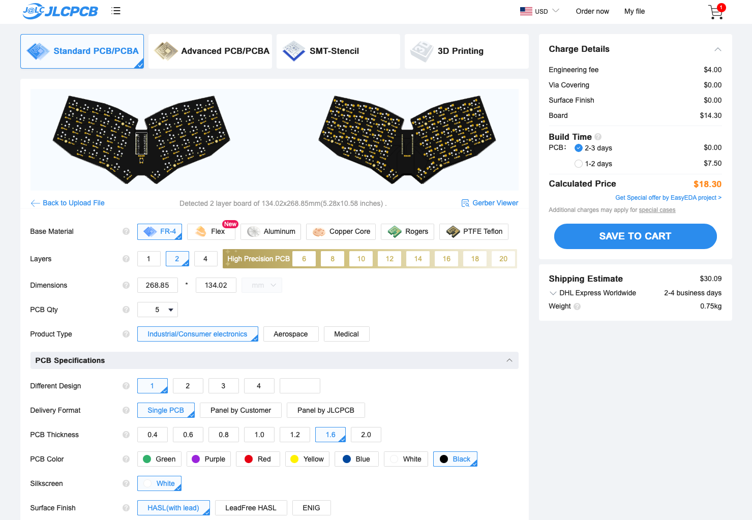
At this point our PCB is ready to fabricate! That's the verb for creating a PCB by the way. The manufacturer of PCBs are known as "Fabricators", or Fabs for short. There's a few popular options out there. JLCPCB and PCBWay are the two large fabricators in China. JLCPCB is known for having competitive prices, particularly if you're making a PCB smaller than 100mm x 100mm. (Not super common for keyboards, but folks have pulled it off.) PCBWay is also another popular Chinese fab. Stateside, OSH Park has made a name for themselves with strikingly purple PCBs. They're a bit more expensive then their overseas counterparts, but they do have a faster turnaround time.
If you decide to create an account with JLCPCB, consider using this URL: https://jlcpcb.com/?from=ERGOGEN It doesn't provide any additional discounts currently, but it'll let JLCPCB know that Ergogen is sending folks their way. If you decide to go with PCBWay, you can use the coupon code ERGOGEN to get 5% off your order. I'm not affiliated with either of these codes, but am more than happy to pass on the Ergogen dev's promo codes.
Whichever fab you go with, the process of getting your PCB manufactured is pretty straightforward. Log into the site, upload your Gerbers (and drill) zip, and then click the buy button. Tutorial finished. Have a great day.
Okay, but seriously. The default options on these sites are fine. You want a 2 layer PCB, a board that's 1.6mm thick, and you can pick whichever color you'd like. There are additional options such as the surface finish that you can adjust for an additional cost, but for your first PCB, you don't need to tweak anything.
One thing worth noting here is that most PCB fabs require a minimum order size. Usually it's around 3-5 PCBs. For this particular example board, JLCPCB will manufacture 5 copies of our PCB for $18 USD, and shipping to the US will cost an additional $15 USD. That's not bad all things considered. Many off the shelf keyboard PCBs run in the $25-35 range. By fabricating your own PCBs, you get some spares in case you have a soldering mishap, or you can share the extras with friends. The manufacturing and shipping of your PCB will take about two weeks, which leaves you just enough time to buy the rest of the parts.
Part Picker
Ordering parts for a keyboard can feel like a balancing act at times. Prices will vary between vendors, but the more places you shop from, the more you'll end up paying in shipping fees.
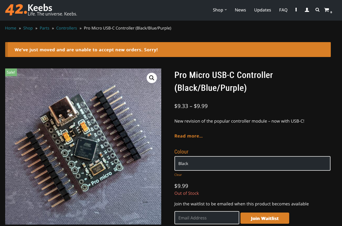
For the keyboard we built, there's a few different parts we need. There's the pre-key components: The Choc switches, the keycaps, and the diodes. There's the microcontroller components: The Arduino Pro Micro, the headers, and the header pins. The OLED screen needs it's own set of pins and headers as well. Finally, there's the ancillary hardware such as the reset button. You'll also need a USB cable if you don't have one already.

Naturally the types of parts you need will vary based on what you're building. If you're making a split keyboard, you'll need a cable to connect the two halves and sockets for the cable to plug into. If you're making a wireless keyboard, you'll need batteries. Looking around at other people's keyboard designs and seeing which designs worked for them can help here.
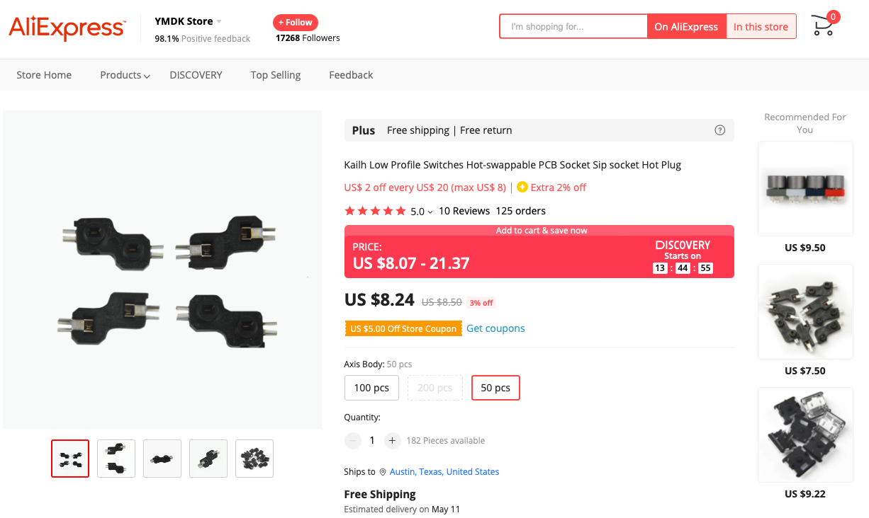
When shopping around, there's a few different stores you can hit up. There's a surprising number of mechanical keyboard vendors out there these days. Companies like 42Keebs, Little Keyboards, and Boardsource are a good place to source keycaps and other keyboard-specific hardware. Electronics component supplies like DigiKey and Mouser are useful resources for picking up the occasional odd button or switch, although their website designs are not beginner friendly. It helps if you know the part number of what you're looking for, and you generally need to be able to read data sheets to double-check you've found the right component. Amazon is always an option as well, although you may not find the best deals there. It's not really worth it to list anything on the site for less than $7-10 USD, so rather than being able to buy a reset button, you may have to buy a bag of 100. Depending on what you need though, it can save you from needing to hit up yet another vendor. Finally, there's Aliexpress. This site is similar to a Chinese version of Amazon's seller marketplace. If you don't mind a two week lead time, you can get some good deals on Choc switches and hotswap sockets there. Your PCBs will take about that long to fab anyways.
After building your keyboard, you may have the realization that your USB cable isn't as spiffy and color coordinated as the ones you see on /r/mechanicalkeyboards. Welcome to your next rabbit hole. If you feel confident enough to solder your own USB cord, Zap Cables can get you the parts needed to make your own custom cable for under $20 USD.
Here's an example part list for our tutorial keyboard. These are also often referred to as a "Bill of Materials", or BOM. All told, you're going to be looking at about $200-300 USD depending on how fancy you want to get with your new keyboard. Hmm, maybe I should have lead with that in the introduction. Surprise? If this isn't your first rodeo, reusing keycaps or leveraging hot swap sockets can at least take some of the sting out.
| Part | Amount | Price (Total) |
|---|---|---|
| PCB Fab (With Shipping) | 1 | $30.00 USD |
| Arduino Pro Micro | 1 | $10.00 USD |
| OLED Display | 1 | $4.00 USD |
| Kailh Choc v2 Switches | 6 (58 Keys Total) | $30.00 USD |
| 1N4148 Diodes (SMD) | 6 (58 Diodes Total) | $2.00 USD |
| Kailh Choc Hotswap Sockets | 6 (58 Sockets Total) | $10.00 USD |
| Reset Switch (SMD, 4 Pin, Flat) | 1 | $0.50 USD |
| Mill Max Sockets & Pins | 1 | $7.50 USD |
| Medium Profile Controller Socket | 1 | $0.50 USD |
| Choc v1 Keycaps | 1 | $75.00 USD |
Firmware Options

Now that all our parts are in the mail, it's time to start thinking about firmware options. DIY mechanical keyboards have a few different firmware options at this point depending on which type of microcontroller you end up using. Most wired Arduino Pro Micro and RP2040 based keyboards use the popular QMK firmware. Meanwhile, wireless keyboards leveraging the Nice!Nano microcontroller typically employ ZMK instead. There are some differences between the two firmwares, but they're both philosophically very similar.
QMK's documentation has a dedicated section for porting your keyboard to QMK. They also have some excellent additional background information on keyboard matrixes. Meanwhile, ZMK's documentation has their own guide for how to create a "shield" configuration for your keyboard. Both of these firmwares rely on you defining the pins used for your rows and columns, and then creating a configuration that outlines the physical arrangement of those keys. From there, you can start programming macros to your heart's content. Both of these firmwares also have support for additional hardware such as the OLED display we created a footprint for earlier. (Although you probably don't want to use an OLED screen on a wireless battery operated keyboard. There's some low power alternatives for those keyboards.)
The two firmwares have slightly different approaches when it comes to compiling your firmware. QMK has instructions on how to compile your new keyboard firmware locally on your computer, while ZMK has a process using GitHub Actions to streamline the compilation of your firmware.
Once you have your firmware compiled, you need to "flash" it onto your keyboard. To start the flashing process, you need to double tap the reset button on your keyboard or microcontroller to reboot the microcontroller into a flashing mode. After that, you need to send the firmware from your computer onto the microcontroller. For sending QMK to an Arduino Pro Micro, this relies on using lower-level commands to send the compiled firmware to the microcontroller. Thankfully the QMK Toolbox utility wraps these functions in a straightforward GUI. ZMK is a bit more straightforward. Double tapping the reset button will mount the Nice!Nano microcontroller as a storage device on your computer. You simply need to drag and drop your compiled firmware onto the microcontroller with your computer's file browser to kick off the flashing process.
Both of these firmwares are well documented with their own community Discords. I might do an article on writing your own QMK or ZMK configuration in the future, but for now their documentation and the row, column, and microcontroller pin background we went over in this guide should be enough to set you down the right path.
Assembling Your Team
Hopefully by the time you've got your first attempt at a custom firmware compiled your parts will have arrived. All that's left is to finally build your keyboard.
Keyboard designs can vary, but the actual act of building them is fairly universal. If this is your first rodeo, find a keyboard with similar functionality to your own and see if it has a build guide. Brian Low did an excellent job outlining the build process for the Sofle Choc for instance. The venerable Corne keyboard has variants for nearly every type of key switch and hotswap socket configuration, so it's also a useful resource for assembly tips. Finally, as much as I've enjoyed writing out this long-form text guide, YouTube does have a place when it comes to soldering tips.
In general, measure twice and solder once. Make sure your parts are oriented properly before you bond it to your PCB with liquid hot metal. You can solder a lot of these parts in any order, but starting with the per-switch components like diodes and hotswap sockets allow you to lay the board flat on your work surface for the first few steps.
You never want to look up nine months after a keyboard build and realize your microcontroller has somehow gone bad, so socket your microcontrollers. It adds a tiny bit onto the cost, but it's worth having the flexibility in the long run. If you get bit by the keyboard building bug, you can even move microcontrollers between keyboards and save yourself a bit of additional cost with each new build.
If you ask a friend to 3D print a case for you, buy them a six pack of their beverage of choice. If you're feeling particularly generous (or are having to iterate through multiple designs), you could even offer to buy your friend a $20 USD spool of 3D printer plastic. It's roughly the cost of mailing away for a piece, and you get to pick your case color rather than dipping into their available supply.
After building your keyboard and gathering the parts for the case, make sure to test your keyboard thoroughly before assembling the case. Enviably you'll notice one lose joint the second you've painstakingly socketed every part and screwed down every piece.
At this point, you should have a brand spanking new keyboard. Thanks for sticking it out through all five parts of this guide! Hopefully you picked up a thing or two!
A Brief Disclaimer
This guide was a fun excuse to learn Ergogen v4. If you'd like to look at any of the config files or outputs from this guide, they're uploaded on Github now. However, I've never actually built this example keyboard. The techniques and methodologies I used in this series are based off of the very similar ChonkV keyboard I made with Ergogen v3. Since they're so similar to one another, I haven't actually sent this particular tutorial PCB design off to get fabricated. There may be a short in the wiring somewhere, or the case may be slightly too snug, or the thumb keys may be brushing up against each other. If you were planning on dropping the Gerbers onto a PCB fab and ordering the parts, just be warned that this hasn't been fully tested in the real world just yet.
If you're not interested in learning Ergogen but like the idea of a Choc-spaced unibody keyboard similar to the Sofle, you're in luck! Josef Adamčík is working on the Stáňa unibody keyboard. It's a more polished, refined take on the style of keyboard that was featured here.
Conclusion
Congratulations, you now have a custom bespoke DIY keyboard unlike any other input device in the world! Happy typing! If you'd like to test your new WPM, MonkeyType is always a popular online typing test.
I sincerely hope you found this guide useful. The world of custom low profile ergonomic mechanical keyboards has been fun to explore, and I hope this series serves as a useful on ramp for those looking to get into the hobby. Even if I didn't cover exactly what you're looking to build here, you hopefully have a better sense of what to Google now. If you designed your own keyboard with this guide, we'd love to hear about it in the Ergogen Discord, or feel free to send me a picture of it on Mastodon! If you're feeling extra generous, I've got a Cash App tip jar.
If you're interested in building a split keyboard, this guide also now features a bonus Part 6 article focusing on reversible split keyboard topics.